
GENERATION OF ELECTRICAL POWER FROM THE FABRIC MADE OF PHOTOVOLTAIC BASED YARNS ........ Patent No:TPE:2012/09041 Çağa BİZİMCAN 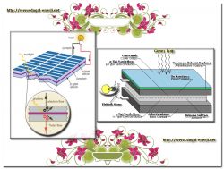 Patent NO.2 TPE-012/09041 Proje yazarı : Çağa Bizimcan SUMMARY
GENERATION OF ELECTRICAL POWER FROM THE FABRIC MADE OF PHOTOVOLTAIC BASED YARNS
Production of silicium and / or the glass fiber yarn from normal or crystalline silicium fibers, and / or normal or crystallized glass fiber or glass wool, continuously or from normal or crystalline 3rd Group intermittently silicium (P-type) and continuously or intermittently from normal or crystalline starting from the 5th Group silicium (N-type) nano-scale up to the highest denier which are obtained by the harmonization of the mono-crystalline or crystalline pure silicium or crystalline pure silicium or crystalline silicium raw material and / or Mono-crystalline or crystalline glass raw material with the 3rd Group and 5th Group elements of the periodic table and / or of the additive compound elements. It is the transmission of the electrical energy obtained by exposure of the natural and artificial light on photovoltaic fabric panels coated by crystal silicium film or by exposure of natural or artificial light without coating made which is made by weaving with the weft density indicated in the photovoltaic cell-based weaving report and the pattern arrangements, together with yarns used in the weft and warp or obtained by knitting having twisted the (P-Type) and (N-type) fibers or glass fiber yarns that are produced with the copper and / or other conductive metal fibers and / or conductive metal filaments in the direction of(S) or (Z) wrapping these yarns around singly or separately to the beams without twisting harmonizing them with the melts of the elements of periodic table that take place in the 3th and 5th groups and making them ready for weaving as raw or as by sizing process on the photovoltaic panels of fabric through copper or conductive wires to batteries and / or to direct transfer of the distribution network.
DESCRIPTION
GENERATION OF ELECTRICAL POWER FROM THE FABRIC MADE OF PHOTOVOLTAIC BASED YARNS
Technical Field The present invention is concerned with producing of direct electrical energy by exposure of sunlight or other artificial and natural light on the photovoltaic cells and actuating them which are created by having weaving copper or other conductive metal filaments along with the produced yarns in the weaving looms and / or knitting machines known in the technique, yarn production using pure crystallized semiconductor molten silicium by doping with any of the elements (P-type) of the 3rd group in the periodic table and again the production of yarns with the crystallized semiconductor pure silicium in the molten form by doping with any of elements of the periodic table of the 5rd group (n-type) weaving these into the fabric panels with maximum tightness.
Previous Technique In the known state of the technique, semiconductor elements particularly the pure crystalline silicon in order for them to be able to be used as a solar cell it is required that they are doped with the elements of the 3rd and 5th group of periodic table. Doping is carried out by adding up the additives taken from the 3rd and 5th group of the periodic table into the pure semiconductor melt in a controlled manner. The type of the doped semiconductor element depends on the type of the atomic structure of the doping element whether (N) or (P). One of elements in the 5th group of the periodic table, for example, phosphorus is added to the melt of pure silicon in order to convert pure crystalline silicium to (N)-type silicium component that is commonly used as the main ingredient of solar cell. Due to the fact that there are 4 electrons in the outer orbit of silicium, and there are 5 electrons in the outer orbit of phosphorus, the extra single electron of phosphorus is given as an electron to the crystal structure of silicon. Therefore 5 group elements are called "Donor" or "N-type" additives, and the doping crystalline silicium is called N-type silicium.
Object of the Invention the problem that this invention aims to solve is the storage into batteries and / or directly transmission to the power distribution network of the directly produced non-polluting electricity obtained in an environmentally friendly way by exposure of the light that is provided by sunlight incoming into our world or by other artificial and natural means onto the photovoltaic panel patterned fabrics that are woven and / or knitted with the (P-Type) and (N-type) yarns which is the invention itself, with the inclusion of other insulating and metal and also nonmetal conductive yarn types that are known in the technique and / or any type of textile into the weaving and knitting.
Description of the Drawings In order for the present invention to accomplish its purpose the fabrics woven and / or knitted by (P-type) and (N-type) yarns that are the present invention, in the form of the photovoltaic cell panels are shown in the attached drawings.
Figure 1 - The perspective aspect view of the woven and / or knitted fabrics from the yarns (P-type) and (n-type) that are the subject of the invention in the form of photovoltaic cell panels in the direction of weft and warp which is the invention itself. Figure 2 - the appearance of the fabric coated by the film that is produced by the raw material of silicium.
Description of the references in the figures 1: Photovoltaic fabric panels woven by (P-type) and (N-type) yarns. 2: Weft part woven by the insulating yarns in the warp yarns direction of the fabric. 3: Warp part woven by the insulating yarns in the weft yarns direction of the fabric. 4: The edge of the fabric that is woven by all copper metal and / or conductive metal yarns or that the copper wire assembled. 5: Copper and / or conductive current wires that provide electron transitions. 6: Copper or conductive metal wires. 7: Film coating made of silicon raw material.
Description of the Invention A-INVENTION IS RELATED WITH THE PRODUCTION OF SILICON AND / OR GLASS FIBER YARN STARTING FROM THE NANO SCALE TO THE HIGHEST DENIER FROM NORMAL OR CRYSTALLIZED SILICON FIBER AND / OR NORMAL OR CRYSTALLIZED GLASS FIBER OR GLASS WOOL NORMAL CONTINUOUS OR INTERMITTENT 3RD GROUP SILICON OR CRYSTALLIZED (P - TYPE) OBTAINED BY THE HARMONIZATION OF PURE OR CHEMICAL COMPOUND OF SUPPLEMENTARY ELEMENTS OF MONO-CRYSTALLIZED OR CRYSTALLIZED PURE SILICON OR SILICON CRYSTALLIZED RAW MATERIALS AND / OR MONO-CRYSTALLIZED OR CRYSTALLIZED GLASS RAW MATERIAL.
It is producing electrical energy directly by activating photovoltaic cells by sunlight or other artificial and natural light Which is the subject of the present invention which is formed by making into woven cloth in maximum tightness with the yarns produced by doping of any of the 3rd group elements of periodic table with molten semi-conductor pure crystalline silicon again with the yarn produced by doping of any of the 5th group elements of periodic table with molten semi-conductor pure crystalline silicon and copper or other conductive metal yarns that will provide the power output. With known methods of the technique pure silicium that is made mono-crystallized or crystallized or silicon element and / or glass raw material in the mono-crystallized or crystallized form is treated for twisting in yarn types of continuous or broken, or other types, by harmonizing with the with pure or composite elements of chemical additives or mixtures from the 3rd group (Boron, aluminum, gallium, indium, thallium, ununtriyum, holmium, Einsteinium) of the periodic table by bringing into pure mono-crystallized and crystalline silicon fibers or mono-crystallized and crystallized glass fibers or wool. Prior to the treatment for twisting from normal or pure crystalline silicon or pure silicon fiber or the crystallized glass fiber, P-type silicon and / or glass fibers and / or after becoming yarn, the treated with molten or solid or others in a mixture of other states with fibers or yarn that is finished and / or blended or coated with One or a portion of or all of the elements of 3rd group in the periodic table of elements. (E.g. boron element and / or other elements in the same group of the periodic table) are added and blended ideal levels. The mixture is obtained with every type of fiber manufacturing apparatus and equipment that are known in the technique with the combination of filaments of round or trilobal-triangular cross-section-in one or more in ideal thickness or nano-sized, where precedent yarn species are numbered to start from the lowest denier and / or nano-scale numbers up to the highest denier yarn is produced. By naming the technical name of this yarn (P-type yarn) or (Crystalline Silicon 3rd Group yarn) or (3rd Group glass yarn) before the twisting and weaving procedure by the pure or in ideal degrees of mixtures of 3rd Group element or elements which are in molten or liquid form having made the heat treatment or coating processes they are formed into coils or reels. The yarn made in coils and reels are ready to be wound on beams after the yarn twisting or with solutions prepared from 3rd Group elements or with liquid complement and ready for weaving after te sizing process.
B-INVENTION IS RELATED WITH THE PRODUCTION OF SILICON AND / OR GLASS FIBER YARN STARTING FROM THE NANO SCALE TO THE HIGHEST DENIER FROM NORMAL OR CRYSTALLIZED SILICON FIBER AND / OR NORMAL OR CRYSTALLIZED GLASS FIBER OR GLASS WOOL NORMAL CONTINUOUS OR INTERMITTENT 3RD GROUP SILICON OR CRYSTALLIZED (P - TYPE) OBTAINED BY THE HARMONIZATION OF PURE OR CHEMICAL COMPOUND OF SUPPLEMENTARY ELEMENTS OF MONO-CRYSTALLIZED OR CRYSTALLIZED PURE SILICON OR SILICON CRYSTALLIZED RAW MATERIALS AND / OR MONO-CRYSTALLIZED OR CRYSTALLIZED GLASS RAW MATERIAL. With known methods of the technique pure silicium that is made mono-crystallized or crystallized or silicon element and / or glass raw material in the mono-crystallized or crystallized form is treated for twisting in yarn types of continuous or broken, or other types, by harmonizing with the with pure or composite elements of chemical additives or mixtures from the 5th group (nitrogen, phosphorus, arsenic, antimony, bismuth, Ununpentium) of the periodic table by bringing into pure mono-crystallized and crystalline silicon fibers or mono-crystallized and crystallized glass fibers or wool. Prior to the treatment for twisting from normal or pure crystalline silicon or pure silicon fiber or the crystallized glass fiber, N-type silicon and / or glass fibers and / or after becoming yarn, the treated with molten or solid or others in a mixture of other states with fibers or yarn that is finished and / or blended or coated with One or a portion of or all of the elements of 5th group in the periodic table of elements. (E.g. Phosphorus element and / or other elements in the same group of the periodic table) are added and blended ideal levels. The mixture is obtained with every type of fiber manufacturing apparatus and equipment that are known in the technique with the combination of filaments of round or trilobal-triangular cross-section-in one or more in ideal thickness or nano-sized, where precedent yarn species are numbered to start from the lowest denier and / or nano-scale numbers up to the highest denier yarn is produced. By naming the technical name of this yarn (N-type yarn) or (Crystalline Silicon 5th Group yarn) or (5th Group glass yarn) before the twisting and weaving procedure by the pure or in ideal degrees of mixtures of 5th Group element or elements which are in molten or liquid form having made the heat treatment or coating processes they are formed into coils or reels. The yarn made in coils and reels are ready to be wound on beams after the twisting or with solutions prepared from 5th Group elements or with their reinforcement or with liquid complement and ready for weaving after the sizing process.
C- THE INVENTION IS CONCERNED WITH MAKING READY FOR WEAVING BY TWISTING THE (P-TYPE) AND (N-TYPE) YARN WITH COPPER AND / OR OTHER CONDUCTIVE METAL FIBERS AND / OR OTHER CONDUCTIVE ELEMENT YARNS IN THE (S) OR (Z) DIRECTIONS OR RAW WITHOUT TWISTING AND / OR WITH THE OPERATION OF THE SIZING.
1) process of weaving by twisting the yarns with each other, where the produced yarns of (P-Type) and (N-type) 3rd and 5th Groups are numbered beginning at the nanoscale to the maximum thickness; With the yarns that are drawn at yarn manufacturing equipments of the known technique and with copper of other conductive metal yarns drawn at yarn manufacturing equipments of the known technique and with and / or other yarns of conductive elements, at the twisting machines of known technique together with in the weaving in the direction of (S) and / or (Z) to be woven at the looms by twisting at a speed that will not make any pilling that are characterized by those deniers it is wound on the beam or beams according to calculated the hackle number and width of the fabric, the tightness of the warp and number of warp threads. By weaving drafting according to the pattern in the weaving report to the weaving machine hackles, placing warped yarns wound on beam or beams in the weaving machines, according to the bobbin case of the weft yarns to the weaving procedure or the thread tightness calculated in accordance with the weaving report in the air looms photovoltaic fabric is woven. The electrical energy transmission is provided to batteries or distribution network having connected the transverse fabric to each other that is made of photovoltaic fabric cells, in series or parallel with the copper or conductive metal wires.
2) processing of knitting yarns as raw; Produced (P-Type) and (N-type) 3rd and 5th Group of the periodic table, starting from the nano scale that the yarns are numbered, to the highest thickness the yarns are produced at the fiber manufacturing devices of the known technique in the knitting machines and labeling machines that are able to knit with all kinds of yarn, in sizes to create photovoltaic panels and are knitted together with the insulating yarns between the panels. So as to form a panel onto the knitted fabrics copper thread or conductive metal threads by putting through strips as stitches connecting photovoltaic fabric panels in series or parallel with these metal yarns to the batteries or distribution network is made that it transmits electrical energy directly.
3) Winding the yarns to the beams individually and weaving operation having weaving drafted; together with the produced (P-Type) and (N-type) yarns, copper or a conductive metal yarns and non-conductive yarns aimed for weaving, in order to be weaved in looms, the hackle numbers determined according to their deniers and calculated according to the width of the fabric and warp tightness, are wound in separate beams in the number of warp wire beam or each yarn type. Warped yarns wound to the beam or individually to beams in the machines of known technique which make sizing process where they are treated with mixtures (P) and (N)-type yarns together with the chemical additives in the 3rd and 5th Group of the periodic table and / or other subjected to sizing treatment with chemical additives that will blend with these chemicals, to the determined hackles according to the width of the fabric and warp tightness copper yarns and other conductive metal fibers and non-conductive yarns aiming to be wound Each beam is placed in a weaving machine in order to be weaving drafted together with the beam it is wound. In addition, according to the detected hackle number and the fabric width by the number of warps to be sorted copper and / or other conductive metal or yarns made of other conductive elements and photovoltaic panels of fabric for the formed edge shown in figure: 1 on any other identified beam, or according to the situation rolled onto the beams on the same hackle together with the beam where (P) and (N) type yarns are wound and made ready to be wound having made having weaving drafted. Prior to weaving, after sizing operation of (P) and (N)-type fibers, it is provided that the sizing additives that take place in the 3rd and 5th Group of the periodic table, conductive copper yarns or other metal fibers come in contact with each other having relaxed for a reasonable period of time and let to dry. According to weaving report copper or conductive metal yarns with (P) type (N) type yarns and non-conductive yarns according to the frequency of the weft so as to form a photovoltaic panel wefted as the weft yarn and the fabric weaving is completed. The photovoltaic panels are connected in series or in parallel with the copper or conductive metal yarns used in the warp and weft that provide the connection of panels with each other.
D-INVENTION IS RELATED WITH THE REPORTING OF INTERMEDIATE INSULATOR AND EDGE CONDUCTOR METAL WEAVING PROCESS WITH PHOTOVOLTAIC FABRIC PANELS. The weaving draft report sequence of the warp yarns wound onto the beams in the weaving procedure shall be in the following order; 1) Weaving draft of warp reporting of Photovoltaic Fabric panels Figure: 1 the sequencing of the (P) and (N)-type fibers that form the panels are made in two different orders. a) (P) and (N)-type fibers and conductive metal threads together or by subjecting to twisting process in the (S) and (Z) direction with conductive fibers in the weaving of photovoltaic panel fabrics with (P) and (N)-type yarns due to the fact that the warp threads are twisted from 3 separate yarns in order for the selected hackle number not to impair the efficiency of weaving it is required that the contact tightness between the wires are provided at the maximum extent. It is the highly efficient production of electricity by touching of sunlight or natural and artificial light onto the panels in the hall to develop inside the photovoltaic panels that will provide a high degree of electron transitions and providing (+) and (-) electrons reach to poles conveniently and easily by providing the number of weft during weaving tightness between the wires at the maximum rate to leave almost no space between the wires. b) it is the efficient production of electricity by subjecting (P) and (N)-type yarns together or separately to the sizing process, by winding them singly or separately to the beams, by making conductive metal fibers warp which are wound on any other beam by weaving drafting with the same hackle, with three separate bobbin cases, with the patterns report which will be determined by the number of wefts in the weaving report of (P), (N) and metal yarns, by weaving having created photovoltaic panels, by ensuring the maximum tightness of the yarn wires, by exposing the natural and artificial light or sunlight on photovoltaic panels, by electron transitions via conductive metal yarns by providing a convenient and easy reach to the (5) (+) and (-) poles in the hall that will be generated in the photovoltaic panels. 2) Weaving drafted in series with the appropriate thicknesses of these yarns or equivalent of non-conductive insulating polyester yarn or other precedent yarn derivatives, the edge warp, forming of the fabric edge of the weaving report detected in the ideal width that is calculated according to the thickness of wires, warp and weft yarns and to begin at the nanoscale up to the highest number together with copper and / or other conductive metal threads. This weaving draft process is applied to both sides of the fabric with the same order. In the sequence, copper and / or other conductive metal yarns are weaving drafted to the outer edge of the fabric. The thicknesses of these conductor yarns and the number of wires in the warp sequence shall be calculated at the resistance to carry the electrical energy produced by photovoltaic panels of the fabric. These copper and / or other conductive metal fibers, for example, the fabric width is 1.52 (1) and it is 3) The forming of photovoltaic part of the solar panels woven fabric is weaving drafted with (P) type and (N) type yarns sequentially at 4) it is the invention of coating photovoltaic fabric panels and a portion or all of the photovoltaic cells that make up the panels by film produced from the silicium raw material (7) starting from the nano-scale to the ideal thickness or with a solution of crystalline silicium or mono-crystalline used in silicium film production by patting over the whole or a part of photovoltaic fabric cells or bonding with silicium-based silicones or on the photovoltaic fabric panels without making any coating and film bonding process on the raw fabric exposing direct sunlight or natural and artificial light onto the produced photovoltaic fabric cells, in the hall that will be generated in photovoltaic fabric panels electron transitions through the copper or conductive metal yarns (5),that generates electricity by providing convenient and easy reaching to the (+) and (-) poles and electrical power transmission to batteries or directly distribution network.
Format of the Implementation of the Invention Industry
Serving to the above-mentioned purposes, that is a renewable energy, which is respectful of the environment and nature, the invention of woven fabric and knitted fabric, which produces electricity and the (P-type yarn) and (N-type yarn) raw materials used in weaving and knitting of this fabric which are the invention itself can be produced, is available in all areas particularly Textile and the energy sector, of industry and / or in any branch of industry and it is has a nature that is applicable to all of the industry.
CLAIMS
1) The invention is yarn production method whereas it is characterized as; In order to obtain semiconductor solar cell elements, in continuous fibers or intermittent type or subjecting other types of yarn to process, harmonizing the mono-crystalline or crystalline pure silicon semiconductor or silicon element and / or glass raw material in mono-crystalline or crystalline form with pure or composite elements of chemical additives or their mixtures with the melt of mono-crystalline and crystalline pure silicon from the 3rd group of the periodic table (Boron, aluminum, gallium, indium, thallium, ununtriyum, holmium, Einsteinium) or mono-crystalline and crystalline glass fiber or ideal levels of wool.
2) It is the method in claim 1 whereas it is characterized as;; Finishing and / or blending, or coating with a mixture in the states of melt or solid or some other with one or some or all of the elements in the 3rd group of the periodic table after it has become into yarn from normal or crystalline pure silicon or pure silicon fibers or crystalline glass fibers, P-type silicon and / or glass fibers or while it is yet in the form of yarn fibers. (E.g. treating, or blending in ideal levels with boron element and / or with other elements in the same group of the periodic table) Together with the mixture that make up the raw material of the (P-type) yarn with every type of fiber manufacturing apparatus and equipment that are known in the technique with the combination of filaments of round or trilobal-triangular cross-section-in one or more in ideal thickness or nano-sized, where precedent yarn species are numbered to start from the lowest denier and / or nano-scale numbers up to the highest denier yarn is produced.
3) The invention is yarn production method whereas it is characterized as; In order to obtain semiconductor solar cell elements, in continuous fibers or intermittent type or subjecting other types of yarn to process for yarn production, harmonizing the mono-crystalline or crystalline pure silicon semiconductor or silicon element and / or glass raw material in mono-crystalline or crystalline form with pure or composite elements of chemical additives or their mixtures with the melt of mono-crystalline and crystalline pure silicon from the 5th group of the periodic table (nitrogen, phosphorus , arsenic, antimony, bismuth, Ununpentium) or that is made mono-crystalline and crystalline glass fiber or ideal levels of wool.
4) It is the method in claim 3 whereas it is characterized as;; Finishing and / or blending, or coating with a mixture in the states of melt or solid or some other with one or some or all of the elements in the 5th group of the periodic table after it has become into yarn from normal or crystalline pure silicon or pure silicon fibers or crystalline glass fibers, N-type silicon and / or glass fibers or while it is yet in the form of yarn fibers. (E.g. treating, or blending in ideal levels with phosphorus element and / or with other elements in the same group of the periodic table ) together with the mixture that make up the raw material of the (N-type) yarn that is obtained with every type of fiber manufacturing apparatus and equipment that are known in the technique with the combination of filaments of round or trilobal-triangular cross-section-in one or more in ideal thickness or nano-sized, where precedent yarn species are numbered to start from the lowest denier and / or nano-scale numbers up to the highest denier yarn is produced.
5) The invention is yarn production method whereas it is characterized as; Bringing yarns produced in Claims 1.2 (P-type) and 3.4 (N-type) and also the yarns from copper and/or other conductive elements known in the technique to a state of ready to be woven by twisting in the (S) or (Z) direction and / or without twisting in a raw state and / or by the process of sizing to be made by warping to beam or beams in according to the weaving report in the context of the invention.
6) It is the method as mentioned in the claims above; It is the weave drafting according to weaving loom hackle pattern at the calculated number of warp wire detected by the deniers of these yarns, the fabric width and warp tightness and also making them ready to be woven together with the yarns obtained in claim 5 that are ready to be woven and with the prepared weaving report according to the hackle number by winding the warped yarns to the beam or beams.
7) It is the method as mentioned in the claims above; To the warp threads introduced into weaving procedure, together with the yarns in the claims of 1 and 2 (P-Type), and claims of 3 and 4, (N-type), calculated in accordance with wire tightness according to the weaving report having made the woven fabric made of photovoltaic panels This pattern is seen in the form of photovoltaic panels in the fabric(P-type) and (N-type) yarns woven All of the Photovoltaic panels of fabric (1) copper metal and / or conductive metal yarns woven or copper wire mounted to the edge of the fabric (4) serial connection in the direction of the warp yarns of the fabric weft woven by the insulating yarns (2) and in the weft direction of the fabric blocking the passage of electrons and between photovoltaic panels of fabric having connected the transverse fabrics that are made by weaving the warp portions with insulating yarns (3) with copper or another conductive metal wires (6) in series or parallel weaving drafted at the edge of fabric in the warp direction it is the transmission of the electricity generated by exposing natural and sunlight or artificial light in the photovoltaic fabric cells on photovoltaic fabric panels to the batteries, or distribution network with copper and / or conductive current wires (5) that provide electron transitions.
8) It is the method as mentioned in the claims above; In the claims of 1 and 2 (P-Type), and claims of 3 and 4, (N-type), yarns produced to the highest thickness, in the knitting machines that make knitting from all types of yarns or in labeling machines in the ideal size to form a photovoltaic cell and knitting together with the insulating yarns that prevent the contact with each other between the cells of photovoltaic panels, and / or with copper or conductive yarns, that provide the photovoltaic cells allowing to come in contact with each other in series or parallel so as to form Photovoltaic Panel, mounting strips in the form of assembly to the sewing and / or knitting fabric with copper thread or conductive metal filaments on the knitted fabrics by connecting photovoltaic cells in series or in parallel with these metal fabric yarns transmission of the electricity, produced by exposing natural and artificial light or sunlight on photovoltaic fabric panels using the electrical wires that are made up with copper or conductive filaments to the batteries, or distribution network.
9) It is the method in the 5th claim; 4) it is the invention of coating photovoltaic fabric panels and a portion or all of the photovoltaic cells that make up the panels by film produced from the silicium raw material (7) starting from the nano-scale to the ideal thickness or with a solution of crystalline silicium or mono-crystalline used in silicium film production by patting over the whole or a part of photovoltaic fabric cells or bonding with silicium-based silicones or on the photovoltaic fabric panels without making any coating and film bonding process on the raw fabric exposing direct sunlight or natural and artificial light onto the produced photovoltaic fabric cells, in the hall that will be generated in photovoltaic fabric panels electron transitions through the copper or conductive metal wires (5) it is the transmission of the generated electricity to batteries or directly distribution network by providing convenient and easy reaching to the (+) and (-) poles. ************************************************** ÖZET FOTOVOLTAİK ESASLI İPLİKLERLE ÜRETİLEN KUMAŞTAN ELEKTRİK ÜRETİMİ Monokristalize veya kristalize saf silisyum veya kristalize saf silisyum veya kristalize silikon hammaddesi ve/veya monokristalize veya kristalize cam hammaddesinin periyodik cetvelin 3.grup ve 5.grup elementleri ve/veya bileşik kimyasal katkı elementlerinin harmonizesinden elde edilen normal veya kristalize silikon elyafı ve/veya normal veya kristalize cam elyafı veya cam yününden devamlı veya kesikli normal veya kristalize 3.grup silikon (P-Tipi) ve devamlı veya kesikli normal veya kristalize 5.grup silikon (N-Tipi) nano ölçekten başlayıp en yüksek denyeye kadar silikon ve/veya cam elyaflı iplik üretilmesi. Üretilen (P-Tipi)ve (N-Tipi) ipliklerin veya cam elyafından ipliklerin bakır ve/veya diğer iletken metal iplikler ve/veya iletken metal ipliklerle (S) veya (Z) yönünde bükülerek veya bu ipliklerin bükülmeden tek veya ayrı ayrı leventlere sarılarak periyodik cetvelin 3.ve 5.grubundan elementlerin içinde bulunan eriyiklerle harmonize edilerek ham veya haşıl işlemi ile dokumaya hazır duruma getirilmesi ile fotovoltaik hücre esaslı dokuma raporu ve desen düzenekleri ile tespit edilen atkı sıklığı ile atkıda ve çözgüde kullanılan ipliklerle dokunması veya örülmesi ile elde edilen fotovoltaik kumaş panelleri üzerine kristal silisyumdan film kaplanarak doğal ve yapay ışık düşürülmesi ve/veya fotovoltaik kumaş panellerine bir kaplama yapılmadan doğal veya yapay ışık düşürülerek elde edilen elektrik enerjisinin bakır veya iletken tellerle akülere ve/veya doğrudan dağıtım şebekesine aktarılmasıdır. 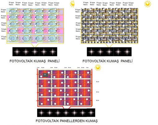 TARİFNAME FOTOVOLTAİK ESASLI İPLİKLERLE ÜRETİLEN KUMAŞTAN ELEKTRİK ÜRETİMİ Teknik Alan Bu buluş, eriyik halindeki yarı iletken kristalize saf silikonla periyodik cetvelin 3.grubundan elementlerin herhangi birinin katkılanması ile (P-Tipi) iplik üretilmesi ve yine eriyik halindeki yarı iletken kristalize saf silikonla periyodik cetvelin 5.grubundaki elementlerin herhangi birinin katkılanması ile (N-Tipi) ipliklerin üretilmesi ve üretilen bu iplikler ile bakır veya diğer metal iletken ipliklerin tekniğin bilinen dokuma tezgahlarında ve/veya örgü makinelerinde azami sıklıkta dokuma kumaş panelleri haline getirilmesi suretiyle oluşturulan fotovoltaik hücrelere güneş ışığı veya diğer yapay ve doğal ışık düşürülerek harekete geçirilmesi suretiyle doğrudan elektrik enerjisi üretilmesi ile ilgilidir. Önceki Teknik Tekniğin bilinen durumunda, Başta kristalize saf Silikon olmak üzere yarı iletken elementlerin güneş pili olarak kullanılabilmeleri için periyodik cetvelin 3.ve 5.grubundan elementler ile katkılanmaları gereklidir. Katkılanma, saf yarı iletken eriyik içerisine peryodik grubun 3.ve 5.grubundan alınan katkı maddelerinin kontrollü olarak eklenmesiyle yapılır. Katkılı yarı iletken elementin (N) ya da (P) tipi olması katkı elementinin atom yapısına bağlıdır. En yaygın güneş pilinin temel maddesi olarak kullanılan kristalize saf silisyumu (N) tipi silisyum bileşenine çevirmek için saf silisyum eriyiğine periyodik cetvelin 5. grubundaki elementlerden biri , örneğin fosfor eklenir. Silisyum’un dış yörüngesinde 4, fosforun dış yörüngesinde 5 elektron olduğu için, fosforun fazla olan tek elektronu Silisyumun kristal yapısına bir elektron verir. Bu nedenle 5. grup elementlerine “verici” ya da “N tipi” katkı maddesi , katkılanan Kristalize Silisyuma ise N tipi Silisyum denir. P tipi silisyum elde etmek için ise, Kristalize saf silisyumdan eriyiğe 3. gruptan bir element , örneğin bor eklenir. Bor elementinin son yörüngesinde 3 elektron olduğu için kristalde bir elektron eksikliği oluşur, bu elektron yokluğuna hol ya da boşluk denir ve pozitif yük taşıdığı gözlemlenir. Bu tür maddelere “P tipi” ya da “alıcı” katkı maddeleri denir. P ya da N tipi ana Kristalize saf silisyumun içerisine gerekli katkı maddelerinin katılması ile yarı iletken eklemler oluşturulur. N tipi yarı iletkende elektronlar, P tipi yarı iletkende holler çoğunluk taşıyıcıdır. P ve N tipi yarı iletkenler organik bir bağ oluşturmadan önce, her iki madde de elektriksel bakımdan nötrdür. Yani P tipinde negatif enerji seviyeleri ile hol sayıları eşit, N tipinde pozitif enerji seviyeleri ile elektron sayıları eşittir. PN eklem oluştuğunda, N tipindeki çoğunluk taşıyıcısı olan elektronlar, P tipine doğru akım oluştururlar. Bu olay her iki tarafta da yük dengesi oluşana kadar devam eder. PN tipi maddenin ara yüzeyinde, yani eklem bölgesinde, P bölgesi tarafında negatif, N bölgesi tarafında pozitif yük birikir. Bu eklem bölgesine “geçiş bölgesi” ya da “yükten arındırılmış bölge” denir. Bu bölgede oluşan elektrik alan “yapısal elektrik alan” olarak adlandırılır. Yarı iletken eklemin güneş pili olarak çalışması için eklem bölgesinde fotovoltaik dönüşümün sağlanması gerekir. Bu dönüşüm iki aşamada olur, ilk aşama, eklem bölgesine ışık düşürülerek elektron-hol çiftleri oluşturulur, ikinci aşamada ise, bunlar bölgedeki elektrik alan yardımıyla birbirlerinden ayrılır. Yarı iletkenler, bir yasak enerji aralığı tarafından ayrılan iki enerji bandından oluşur. Bu bandlar valans bandı ve iletkenlik bandı adını alırlar. Bu yasak enerji aralığına eşit veya daha büyük enerjili bir foton, yarıiletken tarafından soğurulduğu zaman, enerjisini valans banddaki bir elektrona vererek, elektronun iletkenlik bandına çıkmasını sağlar. Böylece, elektron-hol çifti oluşur. Bu olay, PN eklem güneş pilinin ara yüzeyinde meydana gelmiş ise elektron-hol çiftleri buradaki elektrik alan tarafından birbirlerinden ayrılır. Bu şekilde güneş pili, elektronları N bölgesine, holleri de P bölgesine iten bir pompa gibi çalışır. Birbirlerinden ayrılan elektron-hol çiftleri, güneş pilinin uçlarında yararlı bir güç çıkışı oluştururlar. Bu süreç yeniden bir fotonun pil yüzeyine çarpmasıyla aynı şekilde devam eder. Yarı iletkenin iç kısımlarında da, gelen fotonlar tarafından elektron-hol çiftleri oluşturulmaktadır. Fakat gerekli elektrik alan olmadığı için tekrar birleşerek kaybolmaktadırlar. Tekniğin önceki durumunda, cam paneller veya silisyum mikalar halinde üretilen fotovoltaik hücrelerden verimi çok düşük doğrudan elektrik üretilmiştir. Buluşun Amacı Bu buluşun çözümünü amaçladığı problem , dünyamıza gelen güneş ışığı veya diğer yapay ve doğal yollarla sağlanan ışığın,buluş olan (P-Tipi) ve (N-Tipi) ipliklerle dokunan ve/veya örülen fotovoltaik panel desenli kumaş üzerine düşürülerek tekniğin bilinen diğer yalıtkan ve iletken metal ve ametal ve/veya her tür iplik türlerinin de dokumaya ve örgüye dahil edilmesi ile çevreyi kirletmeyen , doğaya saygılı yolla doğrudan doğruya elde edilen elektriğin akülerde depolanması ve/veya doğrudan elektrik dağıtım şebekesine aktarılmasıdır. Şekillerin Açıklaması Bu buluşun amacına ulaşması için buluş olan (P-Tipi) ve (N-Tipi) ipliklerle gerçekleştirilen fotovoltaik hücre panelleri şeklinde dokunmuş ve/veya örülmüş kumaşlar ekli şekillerde gösterilmiştir. Şekil 1- Buluş konusu (P-Tipi) ve (N-Tipi) ipliklerden fotovoltaik hücre panelleri şeklinde buluş olan dokunmuş ve/veya örülmüş kumaşların atkı ve çözgü yönünde en-boy perspektif görünüşüdür. Şekil 2- Kumaşın silisyum hammaddesi ile üretilen filmle kaplanan görünüşü . Şekillerdeki referansların açıklaması 1: (P-Tipi)ve (N-Tipi) ipliklerle dokunan Fotovoltaik kumaş panelleri. 2: Kumaşın çözgü iplik yönünde yalıtkan ipliklerle dokunan atkı kısmı. 3: Kumaşın atkı iplik yönünde yalıtkan ipliklerle dokunan çözgü kısmı. 4: Tamamı bakır metal ve/veya iletken metal ipliklerle dokunan veya bakır tel montajlanan kumaş kenarı. 5: Elektron geçişlerini sağlayan bakır ve/veya iletken akım telleri. 6: Bakır veya iletken metal teller . 7: Silisyum hammaddesinden üretilen film kaplaması. Buluşun Açıklaması A-BULUŞ, MONOKRİSTALİZE VEYA KRİSTALİZE SAF SİLİSYUM VEYA KRİSTALİZE SİLİKON HAMMADDESİ VE /VEYA MONOKRİSTALİZE VEYA KRİSTALİZE CAM HAMMADDESİNİN SAF VEYA BİLEŞİK KİMYASAL KATKI ELEMENTLERİNİN HARMONİZESİNDEN ELDE EDİLEN NORMAL VEYA KRİSTALİZE SİLİKON ELYAFI VE /VEYA NORMAL VEYA KRİSTALİZE CAM ELYAFI VEYA CAM YÜNÜNDEN DEVAMLI VEYA KESİKLİ NORMAL VEYA KRİSTALİZE 3.GRUP SİLİKON (P – TİPİ ) NANO ÖLÇEKTEN BAŞLAYIP EN YÜKSEK DENYEYE KADAR SİLİKON VE/VEYA CAM ELYAFLI İPLİK ÜRETİMİ İLE İLGİLİDİR. Bu buluşun konusunu teşkil eden eriyik halindeki yarı iletken kristalize saf silikonla periyodik cetvelin 3.grubundan elementlerin herhangi birinin katkılanması ile üretilen iplik ile yine eriyik halindeki yarı iletken kristalize saf silikonla periyodik cetvelin 5.grubundaki elementlerin herhangi birinin katkılanması ile üretilen ipliğin ve güç çıkışını sağlayacak bakır veya diğer metal iletken ipliklerin azami sıklıkta dokuma kumaş haline getirilmesi suretiyle oluşturulan fotovoltaik hücrelerin güneş ışığı veya diğer yapay ve doğal ışıklarla harekete geçirilmesi suretiyle doğrudan elektrik enerjisi üretilmesidir. Tekniğin bilinen yöntemleri ile monokristalize veya kristalize hale getirilen saf silisyum veya silikon elementi ve/veya monokristalize veya kristalize haldeki cam hammaddesi , periyodik cetvelin 3. grubundan (Bor, alüminyum, galyum, indiyum, talyum, ununtriyum,holmiyum, aynştaynyum) saf veya bileşik kimyasal katkı elementleri veya karışımı ile harmonize edilerek saf monokristalize ve kristalize silikon elyafı veya monokristalize ve kristalize cam elyafı veya yünü haline getirilerek , devamlı veya kesik tipte veya diğer iplik tiplerinde iplik üretimi için işleme tabi tutulurlar. Normal veya Kristalize saf silisyum veya saf silikon elyafı veya kristalize cam elyafı P-Tipi Silikon ve/veya cam elyafından iplik üretimi için işleme tabi tutulmadan önce ve/veya iplik haline geldikten sonra işleme tabi tutulan elyaf veya ipliğe elementlerin periyodik cetvelin 3. grubundan olan elementlerden biri veya bir kısmının veya tümünün eriyik veya katı veya diğer başka durumlardaki karışımı ile terbiye edilir ve/veya harmanlanır veya kaplanır. (örneğin; Bor elementi ve/veya periyodik cetvelin aynı grubundaki diğer elementler ) ideal ölçülerde eklenir ve harmanlanır. Elde edilen bu karışım tekniğin bilinen her türlü iplik üretim düzenek ve cihazları ile bir veya birden fazla ideal kalınlıkta veya nano ölçülerde yuvarlak veya trilobal –üçgen kesit-filamentlerin bir araya gelmesi ile emsal iplik cinslerinin numaralandırıldığı en düşük denyeden ve/veya nano ölçekli numaralardan başlamak üzere en yüksek denyeye kadar iplik üretilir. Bu ipliğin teknik adının (P-Tipi iplik) veya (Kristalize 3.Grup Silikon iplik)veya (3.Grup cam iplik) olarak adlandırılarak büküm ve dokuma ameliyesinden önce 3.grup element veya elementlerin eriyik veya sıvı halinde olan saf veya karışımlarından ideal derecelerde ısıl işlemlerden veya kaplama işleminden geçirilerek bobin yada çile haline getirilir. Bobin ve çile yapılan iplik büküm veya 3.grup elementlerden hazırlanan eriyik veya sıvı tamamlayıcı ile leventlere sarılmaya ve haşıl işlemi sonrasında dokumaya hazırdır. B-BULUŞ, MONOKRİSTALİZE VEYA KRİSTALİZE SAF SİLİSYUM VEYA KRİSTALİZE SİLİKON HAMMADDESİ VE /VEYA MONOKRİSTALİZE VEYA KRİSTALİZE CAM HAMMADDESİNİN SAF VEYA BİLEŞİK KİMYASAL KATKI ELEMENTLERİNİN HARMONİZESİNDEN ELDE EDİLEN NORMAL VEYA KRİSTALİZE SİLİKON ELYAFI VE /VEYA NORMAL VEYA KRİSTALİZE CAM ELYAFI VEYA CAM YÜNÜNDEN DEVAMLI VEYA KESİKLİ NORMAL VEYA KRİSTALİZE 5.GRUP SİLİKON (N – TİPİ ) NANO ÖLÇEKTEN BAŞLAYIP EN YÜKSEK DENYEYE KADAR SİLİKON VE/VEYA CAM ELYAFLI İPLİK ÜRETİMİ İLE İLGİLİDİR. Tekniğin bilinen yöntemleri ile Monokristalize veya kristalize hale getirilen saf silisyum veya silikon elementi ve/veya monokristalize veya kristalize haldeki cam hammaddesi , periyodik cetvelin 5.grubundan(Azot,fosfor,arsenik,antimon,bizmut,ununpentiyum) saf veya bileşik kimyasal katkı elementleri veya karışımı ile harmonize edilerek saf monokristalize ve kristalize silikon elyafı veya monokristalize ve kristalize cam elyafı veya yünü haline getirilerek , devamlı veya kesik tipte veya diğer iplik tiplerinde iplik üretimi için işleme tabi tutulurlar. Normal veya Kristalize saf silisyum veya saf silikon elyafı veya kristalize cam elyafı N-Tipi Silikon ve/veya cam elyafından iplik üretimi için işleme tabi tutulmadan önce ve/veya iplik haline geldikten sonra işleme tabi tutulan elyaf veya ipliğe elementlerin periyodik cetvelin 5. grubundan olan elementlerden biri veya bir kısmının veya tümünün eriyik veya katı veya diğer başka durumlardaki karışımı ile terbiye edilir ve/veya harmanlanır veya kaplanır. (örneğin; fosfor elementi ve/veya periyodik cetvelin aynı grubundaki diğer elementler ) ideal ölçülerde eklenir ve harmanlanır. Elde edilen bu karışım tekniğin bilinen her türlü iplik üretim düzenek ve cihazları ile bir veya birden fazla ideal kalınlıkta veya nano ölçülerde yuvarlak veya trilobal –üçgen kesit-filamentlerin bir araya gelmesi ile emsal iplik cinslerinin numaralandırıldığı en düşük denyeden ve/veya nano ölçekli numaralardan başlamak üzere en yüksek denyeye kadar iplik üretilir. Bu ipliğin teknik adının (N-Tipi iplik) veya (Kristalize 5.Grup Silikon iplik)veya (5.Grup cam iplik) olarak adlandırılarak büküm ve dokuma ameliyesinden önce 5.grup element veya elementlerin eriyik veya sıvı halinde olan saf veya karışımlarından ideal derecelerde ısıl işlemlerden veya kaplama işleminden geçirilerek bobin yada çile haline getirilir. Bobin ve çile yapılan iplik büküm veya 5.grup elementlerden veya bunların takviyesi ile hazırlanan eriyik veya sıvı tamamlayıcı ile haşıl işlemi ve leventlere sarılma sonrasında dokumaya hazırdır. C- BULUŞ , (P-TİPİ ) VE (N-TİPİ ) İPLİKLERİN BAKIR VE/VEYA DİĞER İLETKEN METAL İPLİKLER VE/VEYA DİĞER İLETKEN ELEMENTLERDEN İPLİKLERİN (S) VEYA (Z) YÖNÜNDE BÜKÜLEREK VEYA BÜKÜLMEDEN HAM HALDE VE/VEYA HAŞIL İŞLEMİ İLE DOKUMAYA HAZIR DURUMA GETİRİLMESİ İLE İLGİLİDİR. 1)İpliklerin birbirleri ile bükülerek dokunması işlemi ; Üretilen (P-Tipi) ve (N-Tipi) 3. ve 5.Grup ipliklerin numaralandırıldığı nano ölçülerden başlamak üzere en yüksek kalınlığa kadar tekniğin bilinen iplik üretim cihazlarında çekilen iplikler ile tekniğin bilinen cihazlarında çekilen bakır ve/veya diğer iletken metal iplikler ve/veya diğer iletken elementlerden iplikler tekniğin bilinen iplik büküm makinelerinde birlikte (S) ve/veya (Z) yönünde dokumada kabarma yapmayacak devirde bükülerek dokuma tezgahlarında dokunmak üzere denyelerine göre tespit edilen tarak numarası ve kumaş eni ile çözgü sıklığına göre hesaplanan çözgü tel adedinde levent veya leventlere sarılır. Levent veya leventlere sarılan çözülmüş iplikler dokuma makinesi taraklarına desene göre dokuma raporu ile taharlanarak dokuma makinelerine yerleştirilerek dokuma ameliyesine atkı ipliklerinin mekikler veya havalı tezgahlarda dokuma raporuna uygun hesaplanan tel sıklığına göre fotovoltaik kumaş dokuması yapılır. Fotovoltaik kumaş hücrelerinin oluşturduğu enleme kumaşlar birbirlerine bakır veya iletken metal tellerle seri yada paralel bağlanarak akülere veya dağıtım şebekesine elektrik enerjisi iletilmesi sağlanır. 2) İpliklerin ham olarak örülmesi işlemi; İpliklerin numaralandırıldığı nano ölçüden başlamak üzere Üretilen (P-Tipi) ve (N-Tipi ) Periyodik cetvelin 3.ve 5.grup en yüksek kalınlığa kadar tekniğin bilinen iplik üretim cihazlarında üretilen iplikler, her türlü iplikten örgü yapan örme makinelerinde veya etiket makinelerinde fotovoltaik panel oluşturacak ölçülerde ve paneller arasında yalıtkan ipliklerle birlikte örülür. Panel oluşturulacak şekilde örülen kumaşlar üzerine bakır iplik veya iletken metal ipliklerle dikiş halinde şeritler geçirilerek bu metal ipliklerle fotovoltaik kumaş panelleri seri yada paralel bağlayarak akülere veya dağıtım şebekesine doğrudan elektrik enerjisi iletilmesi sağlanır. 3) İpliklerin ayrı ayrı leventlere sarılarak ve taharlanarak dokunması işlemi ; Üretilen (P-Tipi) ve (N-Tipi) iplikler ile bakır veya iletken metal iplikler ve iletken olmayan dokumaya matuf iplikler dokuma tezgahlarında dokunmak üzere denyelerine göre tespit edilen tarak numarası ve kumaş eni ile çözgü sıklığına göre hesaplanan çözgü tel adedinde levent veya her iplik tipi ayrı leventlere sarılır. Levent veya ayrı ayrı leventlere sarılan çözülmüş iplikler tekniğin bilinen haşıl işlemi yapan makinelerinde (P) ve (N) tipi ipliklerin karışımları ile terbiye edildikleri 3. ve 5.grup periyodik cetvellerde yazılı kimyasal katkı maddeleri ile ve/veya bu kimyasal maddelerle uyum sağlayan diğer kimyasal katkı maddeleri ile haşıl muamelesine tabi tutularak tespit edilen taraklara kumaş eni ve çözgü sıklığına göre Bakır iplik ve diğer iletken metal iplikler ile iletken olmayan dokumaya matuf ipliklerin birlikte sarıldığı leventle birlikte taharlanmak üzere her bir levent dokuma makinesine yerleştirilir . Ayrıca tespit edilen tarak numarasına ve kumaş enine göre sıralanacak çözgü sayısına göre bakır ve/veya diğer iletken metal veya diğer iletken elementten mamul iplikler ve kumaşın fotovoltaik panellerini şekil:1 oluşturan gösterilen kenarı için tespit edilen başkaca bir levente veya duruma göre leventlere sarılarak aynı tarak üzerinde (P) ve (N) Tipi ipliklerin sarılı olduğu leventle birlikte taharlanarak dokumaya hazır duruma getirilir. (P)ve (N) tipi ipliklerin haşıl işleminden sonra dokuma öncesi makul bir süre dinlendirilip kurumaya bırakılarak 3.ve 5.grup periyodik cetvelde yer alan haşıl katkı maddelerinin birbirleri ve iletken bakır iplik veya diğer metal ipliklerle temas etmemesi sağlanır. Dokuma raporuna göre fotovoltaik panel oluşturacak şekilde atkı sıklığına göre (P) Tipi (N) Tipi ipliklerle bakır veya iletken metal iplikler ve iletken olmayan iplikler atkı ipliği olarak atılır ve kumaşın dokuma işlemi tamamlanır. Fotovoltaik panellerin birbirleri ile bağlantısını sağlayan çözgü ve atkıda kullanılan bakır veya iletken metal ipliklerle paneller seri yada paralel bağlanarak akülere veya dağıtım şebekesine doğrudan elektrik enerjisi iletilmesi sağlanır. D- BULUŞ, FOTOVOLTAİK KUMAŞ PANELLERİ İLE ARA YALITKAN VE KENAR İLETKEN METAL DOKUMA İŞLEMİNİN RAPORLANMASI İLE İLGİLİDİR. Dokuma ameliyesinde leventlere sarılı çözgü ipliklerinin tahar raporu sıralaması aşağıdaki düzende olacaktır; 1)Fotovoltaik Kumaş panellerinin şekil:1çözgü taharının raporlanmasında panelleri oluşturan (P) ve (N)tipi ipliklerin sıralaması iki farklı düzende yapılmaktadır. a) (P) ve (N) tipi ipliklerin ve iletken metal ipliklerin birlikte veya iletken ipliklerle (S)ve (Z) yönünde büküm işlemine tabi tutulması ile (P) ve (N)tipi ipliklerle yapılan fotovoltaik panel kumaşların dokunmasında çözgü ipliklerinin 3 ayrı iplikten bükülmüş olması sebebiyle seçilecek tarak numarasının dokuma randımanını düşürmemesi ve teller arasındaki temas ve sıklığı azami ölçüde sağlaması gerekmektedir. Dokuma sırasında atkı sayısının teller arasındaki sıkılığı da azami ölçüde sağlaması ve teller arasında hemen hiç boşluk bırakılmaması güneş ışığının veya doğal ve yapay ışığın paneller üzerine değmesi ile fotovoltaik paneller içinde oluşacak holde elektron geçişlerini yüksek ölçüde sağlayacak ve elektronların (+) ve (-) kutuplara rahat ve kolay ulaşmasını sağlayarak yüksek verimli elektrik üretilmesidir. b) (P)ve (N) tipi ipliklerin birlikte veya ayrı ayrı haşıl işlemine tabi tutularak tek veya ayrı ayrı leventlere sarılarak başkaca levente sarılı iletken metal ipliklerin aynı tarakta taharlanarak çözgü haline getirilmesi ile üç ayrı mekikle (P) , (N) ve Metal ipliklerin dokuma raporundaki atkı sayılarına göre tespit edilecek desen raporuyla fotovoltaik panellerin oluşturularak dokunması ile iplik teller arasında azami sıklığın sağlanması suretiyle güneş ışığının veya doğal ve yapay ışığın fotovoltaik paneller üzerine düşürülerek fotovoltaik panellerde oluşacak holde elektron geçişlerini iletken metal iplikler vasıtasıyla (5) (+) ve (-) kutuplara rahat ve kolay ulaşmasını sağlayarak verimli elektrik üretilmesidir. 2)İdeal genişlikte tespit edilen dokuma raporunun kumaş kenarını oluşturan kenar çözgü telleri , atkı ve çözgü ipliklerinin kalınlığına göre hesaplanan ve nano ölçüden başlamak üzere en yüksek numaraya kadar bakır ve/ veya diğer iletken metal ipliklerle bu ipliklerin kalınlıklarına uygun veya eşdeğerde iletken olmayan yalıtkan polyester iplik veya diğer emsal iplik türevleri ile sıralı olarak taharlanır. Bu taharlanma işlemi kumaşın her iki kenarına aynı sıralama ile uygulanır. Sıralamada , kumaş kenarının en dışında bakır ve/ veya diğer iletken metal iplikler taharlanır.Bu iletken ipliklerin kalınlıkları ve çözgü sıralamasındaki tel sayısı fotovoltaik kumaş panellerinin ürettiği elektrik enerjisini taşıyacak dirençte hesaplanacaktır. Bu bakır ve/ veya diğer iletken metal ipliklerin , örneğin ; 1.52 kumaş eni olan (1) ve 3)Kumaşın fotovoltaik kısmını oluşturan güneş panellerinin dokuması ise diğer başka ideal genişlikte (P) tipi ve (N) tipi ipliklerle sıralı olarak taharlanır. 4) Fotovoltaik kumaş panelleri ve bu panelleri oluşturan fotovoltaik hücrelerin tamamı veya bir kısmı nano ölçekten başlayıp ideal kalınlığa kadar silisyum hammaddesinden üretilen film kaplanarak (7) veya silisyum filminin üretiminde kullanılan kristalize veya monokristalize silisyum eriğiyi ile fotovoltaik kumaş hücrelerinin tamamının veya bir kısmının üzerleri sıvazlanarak veya silisyum esaslı silikonlarla yapıştırılarak veya fotovoltaik kumaş panelleri üzerinde hiçbir kaplama ve film yapıştırma işlemi yapmadan ham kumaş üzerine doğrudan güneş ışığının veya doğal ve yapay ışığın üretilen fotovoltaik kumaş hücreleri üzerine düşürülerek fotovoltaik kumaş panellerinde oluşacak holde elektron geçişlerini bakır veya iletken metal iplikler vasıtasıyla (5) , (+)ve (-) kutuplara rahat ve kolay ulaşmasını sağlayarak elektrik üreten ve akülere veya dağıtım şebekesine doğrudan elektrik enerjisi iletilmesini sağlayan buluştur. Buluşun Sanayiye Uygulanma Biçimi Yukarıda bahsedilen amaçlara hizmet eden , çevreye ve doğaya saygılı yenilenebilir enerji olan elektriği üreten buluş olan dokuma kumaş ve örgü kumaş ve bu kumaşın dokunması ve örülmesinde kullanılan buluş olan (P-Tipi iplik) ve (N-Tipi iplik) hammaddeleri Sanayinin başta Tekstil ve Enerji sektöründe ve/veya sanayinin herhangi bir dalında üretilebilir ve her alanda kullanılabilir olup, sanayiye uygulanabilir yapıdadır. 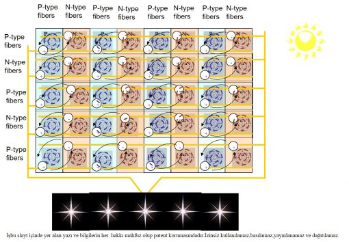 İSTEMLER 1)Buluş, iplik üretim yöntemi olup özelliği ; Yarı iletken monokristalize veya kristalize saf silisyum veya silikon elementi ve/veya monokristalize veya kristalize haldeki cam hammaddesi olmak üzere yarı iletken elementlerden güneş pili elde etmek için, periyodik cetvelin 3.grubundan (Bor, alüminyum, galyum, indiyum, talyum, ununtriyum, holmiyum, aynştaynyum) saf veya bileşik kimyasal katkı elementleri veya karışımı ile saf monokristalize ve kristalize silikon eriği veya monokristalize ve kristalize cam elyafı veya yünü ideal ölçülerde harmonize edilerek devamlı elyaf veya kesik elyaf tipinde veya diğer iplik tiplerinde işleme tabi tutulmasıdır. 2) İstem 1’deki yöntem olup özelliği ; Normal veya Kristalize saf silisyum veya saf silikon elyafı veya kristalize cam elyafı P-Tipi Silikon ve/veya cam elyafından iplik haline geldikten sonra veya henüz iplik elyafı halinde iken , periyodik cetvelin 3. grubundan olan elementlerden biri veya bir kısmının veya tümünün eriyik veya katı veya diğer başka durumlardaki karışımı ile terbiye edilmesi ve/veya harmanlanması veya kaplanması. (örneğin; Bor elementi ve/veya periyodik cetvelin aynı grubundaki diğer elementlerle ideal ölçülerde terbiye edilmesi veya harmanlanması) . (P-Tipi) ipliğin hammaddesini oluşturan karışımla tekniğin bilinen her türlü iplik üretim düzenek ve cihazları ile bir veya birden fazla ideal kalınlıkta veya nano ölçülerde yuvarlak veya trilobal –üçgen kesit-filamentlerin bir araya gelmesi ile üretilen ipliğin emsal iplik cinslerinin numaralandırıldığı en düşük denyeden ve/veya nano ölçekli numaralardan başlamak üzere en yüksek denyeye kadar fotovoltaik esaslı ipliği içermesidir. 3) Buluş iplik üretim yöntemi olup özelliği ; Yarı iletken monokristalize veya kristalize hale getirilen saf silisyum veya silikon elementi ve/veya monokristalize veya kristalize haldeki cam hammaddesi olmak üzere yarı iletken elementlerden güneş pili elde etmek için , periyodik cetvelin 5.grubundan (Azot,fosfor,arsenik,antimon,bizmut,ununpentiyum) saf veya bileşik kimyasal katkı elementleri veya karışımı ile saf monokristalize ve kristalize silikon eriğiyi veya monokristalize ve kristalize cam elyafı veya yünü ideal ölçülerde harmonize edilerek , devamlı elyaf veya kesik elyaf tipinde veya diğer iplik tiplerinde iplik üretimi için işleme tabi tutulmasıdır. 4) İstem 3’deki yöntem olup özelliği; Normal veya Kristalize saf silisyum veya saf silikon elyafı veya kristalize cam elyafı N-Tipi Silikon ve/veya cam elyafından iplik haline geldikten sonra veya henüz iplik elyafı halinde iken , periyodik cetvelin 5. grubundan olan elementlerden biri veya bir kısmının veya tümünün eriyik veya katı veya diğer başka durumlardaki karışımı ile terbiye edilmesi ve/veya harmanlanması veya kaplanması. (örneğin; Fosfor elementi ve/veya periyodik cetvelin aynı grubundaki diğer elementlerle ideal ölçülerde terbiye edilmesi veya harmanlanması) . Buluş olarak elde edilen (N-Tipi) ipliğin hammaddesini oluşturan karışımla tekniğin bilinen her türlü iplik üretim düzenek ve cihazları ile bir veya birden fazla ideal kalınlıkta veya nano ölçülerde yuvarlak veya trilobal –üçgen kesit-filamentlerin bir araya gelmesi ile üretilen bu ipliğin emsal iplik cinslerinin numaralandırıldığı en düşük denyeden ve/veya nano ölçekli numaralardan başlamak üzere en yüksek denyeye kadar fotovoltaik esaslı ipliği içermesidir. 5) Buluş iplik üretim yöntemi olup özelliği ; İstem 1,2’de (P-TİPİ) ve 3,4’de(N-TİPİ) üretilen ipliklerin ve ayrıca tekniğin bilinen Bakır ve/veya diğer iletken elementlerden ipliklerle , (S) veya (Z) yönünde bükülerek ve/veya bükülmeden ham halde ve/veya yapılacak haşıl işlemi ile levent veya leventlere buluş kapsamındaki dokuma raporuna uygun çözülerek dokumaya hazır duruma getirilmesidir. 6) Yukarıdaki istemlerde bahsedilen yöntem olup özelliği ; İstem 5’de elde edilen dokumaya hazır durumdaki ipliklerin ve ayrıca dokumaya hazır duruma gelmesi ile hazırlanan dokuma raporu ile bu ipliklerin denyelerine göre tespit edilen tarak numarası ve kumaş eni ile çözgü sıklığına göre hesaplanan çözgü tel adedinde çözülmüş ipliklerin levent veya leventlere sarılarak dokuma makinesi taraklarına desene göre taharlanmasıdır. 7) Yukarıdaki istemlerde bahsedilen yöntem olup özelliği ; Dokuma ameliyesine sokulan çözgü ipliklerine , 1 ve 2 istemlerdeki (P-Tipi) ve 3 ve 4 istemlerdeki (N-Tipi)iplikler ile Bakır veya diğer iletken iplikler ve yalıtkan atkı ipliklerinin tekniğin bilinen dokuma tezgahlarında mekikli veya havalı veya diğer şekillerde çalışan tezgahlarda dokuma raporuna uygun hesaplanan tel sıklığına göre fotovoltaik kumaş panel dokuması yapılarak bu kumaş içinde fotovoltaik panel deseni şeklinde görülen (P-Tipi) ve (N-Tipi) ipliklerle dokunan Fotovoltaik kumaş panellerinin (1) tamamı bakır metal ve/veya iletken metal ipliklerle dokunan veya bakır tel montajlanan kumaş kenarı (4) seri bağlantısından ve fotovoltaik kumaş panelleri arasında elektronların geçişini engelleyici kumaşın çözgü iplik yönünde yalıtkan ipliklerle dokunan atkı (2) ve kumaşın atkı iplik yönünde yalıtkan ipliklerle dokunan çözgü kısımlarının (3) dokumasıyla oluşan enleme kumaşlar birbirlerine bakır veya iletken metal tellerle (6) seri yada paralel bağlanarak fotovoltaik kumaş panelleri üzerine güneş ışığı veya doğal ve yapay ışık düşürülerek fotovoltaik kumaş hücrelerinde üretilen elektriğin kumaş kenarından çözgü yönünde taharlanan elektron geçişlerini sağlayan bakır ve/veya iletken akım telleri (5) ile akülere veya dağıtım şebekesine iletilmesidir. 8) Yukarıdaki istemlerde bahsedilen yöntem olup özelliği ; 1 ve 2 istemlerdeki (P-Tipi) ve 3 ve 4 istemlerdeki (N-Tipi ) en yüksek kalınlığa kadar üretilen iplikler, her türlü iplikten örgü yapan örme makinelerinde veya etiket makinelerinde fotovoltaik hücre oluşturacak ideal ölçülerde ve fotovoltaik paneller arasında hücrelerin birbirleri ile temasını engelleyen yalıtkan ipliklerle ve/veya fotovoltaik hücrelerin seri veya paralel birbirine temasını sağlayan bakır veya iletken ipliklerle birlikte örülmesi, Fotovoltaik Panel oluşturulacak şekilde örülen kumaşlar üzerine bakır iplik veya iletken metal ipliklerle dikiş ve/veya örgü kumaşa örme şeklinde montaj halinde şeritler geçirilerek bu metal ipliklerle fotovoltaik kumaş hücrelerini seri ya da paralel bağlayarak fotovoltaik kumaş panelleri üzerine güneş ışığı veya doğal ve yapay ışık düşürülerek üretilen elektriğin bakır veya iletken ipliklerin oluşturduğu akım telleri ile akülere veya dağıtım şebekesine iletilmesidir. 9) 5.istemdeki yöntem olup özelliği ; Fotovoltaik kumaş panelleri ve bu panelleri oluşturan fotovoltaik hücrelerin tamamı veya bir kısmı nano ölçekten başlayıp ideal kalınlığa kadar silisyum hammaddesinden üretilen film kaplanarak (7) veya silisyum filminin üretiminde kullanılan kristalize veya monokristalize silisyum eriği ile fotovoltaik kumaş hücrelerinin tamamının veya bir kısmının üzerleri sıvazlanarak veya silisyum esaslı silikonlarla yapıştırılarak veya fotovoltaik kumaş panelleri üzerinde hiçbir kaplama ve film yapıştırma işlemi yapmadan ham kumaş üzerine doğrudan güneş ışığının veya doğal ve yapay ışığın üretilen fotovoltaik kumaş hücreleri üzerine düşürülerek fotovoltaik kumaş panellerinde oluşacak holde elektron geçişlerini sağlayan bakır ve/veya iletken akım telleri (5) vasıtasıyla (+) ve (-) kutuplara ulaşmasını sağlayarak üretilen elektriğin akülere veya dağıtım şebekesine iletilmesidir. 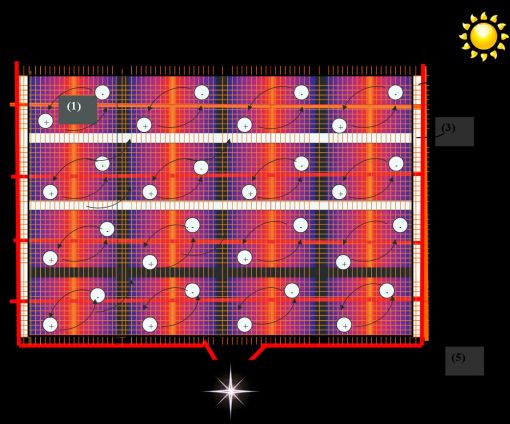 İşbu sayfa ve eklentisi olan dosyalarda yayınlanan projeler Tubitak patent teşviki ve patent koruması kapsamında olup,lisanslıdır. Bu projelerin izinsiz kullanılması,yayınlanması,dağıtılması ve alıntı yapılması yasaktır.Bu kurallara uymayanlar en ağır şekilde tazminat ve cezai yaptırımlarla cezalandırılır.
SUMMARY
GENERATION OF ELECTRICAL POWER FROM THE FABRIC MADE OF PHOTOVOLTAIC BASED YARNS
Production of silicium and / or the glass fiber yarn from normal or crystalline silicium fibers, and / or normal or crystallized glass fiber or glass wool, continuously or from normal or crystalline 3rd Group intermittently silicium (P-type) and continuously or intermittently from normal or crystalline starting from the 5th Group silicium (N-type) nano-scale up to the highest denier which are obtained by the harmonization of the mono-crystalline or crystalline pure silicium or crystalline pure silicium or crystalline silicium raw material and / or Mono-crystalline or crystalline glass raw material with the 3rd Group and 5th Group elements of the periodic table and / or of the additive compound elements. It is the transmission of the electrical energy obtained by exposure of the natural and artificial light on photovoltaic fabric panels coated by crystal silicium film or by exposure of natural or artificial light without coating made which is made by weaving with the weft density indicated in the photovoltaic cell-based weaving report and the pattern arrangements, together with yarns used in the weft and warp or obtained by knitting having twisted the (P-Type) and (N-type) fibers or glass fiber yarns that are produced with the copper and / or other conductive metal fibers and / or conductive metal filaments in the direction of(S) or (Z) wrapping these yarns around singly or separately to the beams without twisting harmonizing them with the melts of the elements of periodic table that take place in the 3th and 5th groups and making them ready for weaving as raw or as by sizing process on the photovoltaic panels of fabric through copper or conductive wires to batteries and / or to direct transfer of the distribution network. GENERATION OF ELECTRICAL POWER FROM THE FABRIC MADE OF PHOTOVOLTAIC BASED YARNS
Technical Field The present invention is concerned with producing of direct electrical energy by exposure of sunlight or other artificial and natural light on the photovoltaic cells and actuating them which are created by having weaving copper or other conductive metal filaments along with the produced yarns in the weaving looms and / or knitting machines known in the technique, yarn production using pure crystallized semiconductor molten silicium by doping with any of the elements (P-type) of the 3rd group in the periodic table and again the production of yarns with the crystallized semiconductor pure silicium in the molten form by doping with any of elements of the periodic table of the 5rd group (n-type) weaving these into the fabric panels with maximum tightness.
Previous Technique In the known state of the technique, semiconductor elements particularly the pure crystalline silicon in order for them to be able to be used as a solar cell it is required that they are doped with the elements of the 3rd and 5th group of periodic table. Doping is carried out by adding up the additives taken from the 3rd and 5th group of the periodic table into the pure semiconductor melt in a controlled manner. The type of the doped semiconductor element depends on the type of the atomic structure of the doping element whether (N) or (P). One of elements in the 5th group of the periodic table, for example, phosphorus is added to the melt of pure silicon in order to convert pure crystalline silicium to (N)-type silicium component that is commonly used as the main ingredient of solar cell. Due to the fact that there are 4 electrons in the outer orbit of silicium, and there are 5 electrons in the outer orbit of phosphorus, the extra single electron of phosphorus is given as an electron to the crystal structure of silicon. Therefore 5 group elements are called "Donor" or "N-type" additives, and the doping crystalline silicium is called N-type silicium.
Object of the Invention the problem that this invention aims to solve is the storage into batteries and / or directly transmission to the power distribution network of the directly produced non-polluting electricity obtained in an environmentally friendly way by exposure of the light that is provided by sunlight incoming into our world or by other artificial and natural means onto the photovoltaic panel patterned fabrics that are woven and / or knitted with the (P-Type) and (N-type) yarns which is the invention itself, with the inclusion of other insulating and metal and also nonmetal conductive yarn types that are known in the technique and / or any type of textile into the weaving and knitting.
Description of the Drawings In order for the present invention to accomplish its purpose the fabrics woven and / or knitted by (P-type) and (N-type) yarns that are the present invention, in the form of the photovoltaic cell panels are shown in the attached drawings.
Figure 1 - The perspective aspect view of the woven and / or knitted fabrics from the yarns (P-type) and (n-type) that are the subject of the invention in the form of photovoltaic cell panels in the direction of weft and warp which is the invention itself. Figure 2 - the appearance of the fabric coated by the film that is produced by the raw material of silicium.
Description of the references in the figures 1: Photovoltaic fabric panels woven by (P-type) and (N-type) yarns. 2: Weft part woven by the insulating yarns in the warp yarns direction of the fabric. 3: Warp part woven by the insulating yarns in the weft yarns direction of the fabric. 4: The edge of the fabric that is woven by all copper metal and / or conductive metal yarns or that the copper wire assembled. 5: Copper and / or conductive current wires that provide electron transitions. 6: Copper or conductive metal wires. 7: Film coating made of silicon raw material.
Description of the Invention A-INVENTION IS RELATED WITH THE PRODUCTION OF SILICON AND / OR GLASS FIBER YARN STARTING FROM THE NANO SCALE TO THE HIGHEST DENIER FROM NORMAL OR CRYSTALLIZED SILICON FIBER AND / OR NORMAL OR CRYSTALLIZED GLASS FIBER OR GLASS WOOL NORMAL CONTINUOUS OR INTERMITTENT 3RD GROUP SILICON OR CRYSTALLIZED (P - TYPE) OBTAINED BY THE HARMONIZATION OF PURE OR CHEMICAL COMPOUND OF SUPPLEMENTARY ELEMENTS OF MONO-CRYSTALLIZED OR CRYSTALLIZED PURE SILICON OR SILICON CRYSTALLIZED RAW MATERIALS AND / OR MONO-CRYSTALLIZED OR CRYSTALLIZED GLASS RAW MATERIAL.
It is producing electrical energy directly by activating photovoltaic cells by sunlight or other artificial and natural light Which is the subject of the present invention which is formed by making into woven cloth in maximum tightness with the yarns produced by doping of any of the 3rd group elements of periodic table with molten semi-conductor pure crystalline silicon again with the yarn produced by doping of any of the 5th group elements of periodic table with molten semi-conductor pure crystalline silicon and copper or other conductive metal yarns that will provide the power output. With known methods of the technique pure silicium that is made mono-crystallized or crystallized or silicon element and / or glass raw material in the mono-crystallized or crystallized form is treated for twisting in yarn types of continuous or broken, or other types, by harmonizing with the with pure or composite elements of chemical additives or mixtures from the 3rd group (Boron, aluminum, gallium, indium, thallium, ununtriyum, holmium, Einsteinium) of the periodic table by bringing into pure mono-crystallized and crystalline silicon fibers or mono-crystallized and crystallized glass fibers or wool. Prior to the treatment for twisting from normal or pure crystalline silicon or pure silicon fiber or the crystallized glass fiber, P-type silicon and / or glass fibers and / or after becoming yarn, the treated with molten or solid or others in a mixture of other states with fibers or yarn that is finished and / or blended or coated with One or a portion of or all of the elements of 3rd group in the periodic table of elements. (E.g. boron element and / or other elements in the same group of the periodic table) are added and blended ideal levels. The mixture is obtained with every type of fiber manufacturing apparatus and equipment that are known in the technique with the combination of filaments of round or trilobal-triangular cross-section-in one or more in ideal thickness or nano-sized, where precedent yarn species are numbered to start from the lowest denier and / or nano-scale numbers up to the highest denier yarn is produced. By naming the technical name of this yarn (P-type yarn) or (Crystalline Silicon 3rd Group yarn) or (3rd Group glass yarn) before the twisting and weaving procedure by the pure or in ideal degrees of mixtures of 3rd Group element or elements which are in molten or liquid form having made the heat treatment or coating processes they are formed into coils or reels. The yarn made in coils and reels are ready to be wound on beams after the yarn twisting or with solutions prepared from 3rd Group elements or with liquid complement and ready for weaving after te sizing process.
B-INVENTION IS RELATED WITH THE PRODUCTION OF SILICON AND / OR GLASS FIBER YARN STARTING FROM THE NANO SCALE TO THE HIGHEST DENIER FROM NORMAL OR CRYSTALLIZED SILICON FIBER AND / OR NORMAL OR CRYSTALLIZED GLASS FIBER OR GLASS WOOL NORMAL CONTINUOUS OR INTERMITTENT 3RD GROUP SILICON OR CRYSTALLIZED (P - TYPE) OBTAINED BY THE HARMONIZATION OF PURE OR CHEMICAL COMPOUND OF SUPPLEMENTARY ELEMENTS OF MONO-CRYSTALLIZED OR CRYSTALLIZED PURE SILICON OR SILICON CRYSTALLIZED RAW MATERIALS AND / OR MONO-CRYSTALLIZED OR CRYSTALLIZED GLASS RAW MATERIAL. With known methods of the technique pure silicium that is made mono-crystallized or crystallized or silicon element and / or glass raw material in the mono-crystallized or crystallized form is treated for twisting in yarn types of continuous or broken, or other types, by harmonizing with the with pure or composite elements of chemical additives or mixtures from the 5th group (nitrogen, phosphorus, arsenic, antimony, bismuth, Ununpentium) of the periodic table by bringing into pure mono-crystallized and crystalline silicon fibers or mono-crystallized and crystallized glass fibers or wool. Prior to the treatment for twisting from normal or pure crystalline silicon or pure silicon fiber or the crystallized glass fiber, N-type silicon and / or glass fibers and / or after becoming yarn, the treated with molten or solid or others in a mixture of other states with fibers or yarn that is finished and / or blended or coated with One or a portion of or all of the elements of 5th group in the periodic table of elements. (E.g. Phosphorus element and / or other elements in the same group of the periodic table) are added and blended ideal levels. The mixture is obtained with every type of fiber manufacturing apparatus and equipment that are known in the technique with the combination of filaments of round or trilobal-triangular cross-section-in one or more in ideal thickness or nano-sized, where precedent yarn species are numbered to start from the lowest denier and / or nano-scale numbers up to the highest denier yarn is produced. By naming the technical name of this yarn (N-type yarn) or (Crystalline Silicon 5th Group yarn) or (5th Group glass yarn) before the twisting and weaving procedure by the pure or in ideal degrees of mixtures of 5th Group element or elements which are in molten or liquid form having made the heat treatment or coating processes they are formed into coils or reels. The yarn made in coils and reels are ready to be wound on beams after the twisting or with solutions prepared from 5th Group elements or with their reinforcement or with liquid complement and ready for weaving after the sizing process.
C- THE INVENTION IS CONCERNED WITH MAKING READY FOR WEAVING BY TWISTING THE (P-TYPE) AND (N-TYPE) YARN WITH COPPER AND / OR OTHER CONDUCTIVE METAL FIBERS AND / OR OTHER CONDUCTIVE ELEMENT YARNS IN THE (S) OR (Z) DIRECTIONS OR RAW WITHOUT TWISTING AND / OR WITH THE OPERATION OF THE SIZING.
1) process of weaving by twisting the yarns with each other, where the produced yarns of (P-Type) and (N-type) 3rd and 5th Groups are numbered beginning at the nanoscale to the maximum thickness; With the yarns that are drawn at yarn manufacturing equipments of the known technique and with copper of other conductive metal yarns drawn at yarn manufacturing equipments of the known technique and with and / or other yarns of conductive elements, at the twisting machines of known technique together with in the weaving in the direction of (S) and / or (Z) to be woven at the looms by twisting at a speed that will not make any pilling that are characterized by those deniers it is wound on the beam or beams according to calculated the hackle number and width of the fabric, the tightness of the warp and number of warp threads. By weaving drafting according to the pattern in the weaving report to the weaving machine hackles, placing warped yarns wound on beam or beams in the weaving machines, according to the bobbin case of the weft yarns to the weaving procedure or the thread tightness calculated in accordance with the weaving report in the air looms photovoltaic fabric is woven. The electrical energy transmission is provided to batteries or distribution network having connected the transverse fabric to each other that is made of photovoltaic fabric cells, in series or parallel with the copper or conductive metal wires.
2) processing of knitting yarns as raw; Produced (P-Type) and (N-type) 3rd and 5th Group of the periodic table, starting from the nano scale that the yarns are numbered, to the highest thickness the yarns are produced at the fiber manufacturing devices of the known technique in the knitting machines and labeling machines that are able to knit with all kinds of yarn, in sizes to create photovoltaic panels and are knitted together with the insulating yarns between the panels. So as to form a panel onto the knitted fabrics copper thread or conductive metal threads by putting through strips as stitches connecting photovoltaic fabric panels in series or parallel with these metal yarns to the batteries or distribution network is made that it transmits electrical energy directly.
3) Winding the yarns to the beams individually and weaving operation having weaving drafted; together with the produced (P-Type) and (N-type) yarns, copper or a conductive metal yarns and non-conductive yarns aimed for weaving, in order to be weaved in looms, the hackle numbers determined according to their deniers and calculated according to the width of the fabric and warp tightness, are wound in separate beams in the number of warp wire beam or each yarn type. Warped yarns wound to the beam or individually to beams in the machines of known technique which make sizing process where they are treated with mixtures (P) and (N)-type yarns together with the chemical additives in the 3rd and 5th Group of the periodic table and / or other subjected to sizing treatment with chemical additives that will blend with these chemicals, to the determined hackles according to the width of the fabric and warp tightness copper yarns and other conductive metal fibers and non-conductive yarns aiming to be wound Each beam is placed in a weaving machine in order to be weaving drafted together with the beam it is wound. In addition, according to the detected hackle number and the fabric width by the number of warps to be sorted copper and / or other conductive metal or yarns made of other conductive elements and photovoltaic panels of fabric for the formed edge shown in figure: 1 on any other identified beam, or according to the situation rolled onto the beams on the same hackle together with the beam where (P) and (N) type yarns are wound and made ready to be wound having made having weaving drafted. Prior to weaving, after sizing operation of (P) and (N)-type fibers, it is provided that the sizing additives that take place in the 3rd and 5th Group of the periodic table, conductive copper yarns or other metal fibers come in contact with each other having relaxed for a reasonable period of time and let to dry. According to weaving report copper or conductive metal yarns with (P) type (N) type yarns and non-conductive yarns according to the frequency of the weft so as to form a photovoltaic panel wefted as the weft yarn and the fabric weaving is completed. The photovoltaic panels are connected in series or in parallel with the copper or conductive metal yarns used in the warp and weft that provide the connection of panels with each other.
D-INVENTION IS RELATED WITH THE REPORTING OF INTERMEDIATE INSULATOR AND EDGE CONDUCTOR METAL WEAVING PROCESS WITH PHOTOVOLTAIC FABRIC PANELS. The weaving draft report sequence of the warp yarns wound onto the beams in the weaving procedure shall be in the following order; 1) Weaving draft of warp reporting of Photovoltaic Fabric panels Figure: 1 the sequencing of the (P) and (N)-type fibers that form the panels are made in two different orders. a) (P) and (N)-type fibers and conductive metal threads together or by subjecting to twisting process in the (S) and (Z) direction with conductive fibers in the weaving of photovoltaic panel fabrics with (P) and (N)-type yarns due to the fact that the warp threads are twisted from 3 separate yarns in order for the selected hackle number not to impair the efficiency of weaving it is required that the contact tightness between the wires are provided at the maximum extent. It is the highly efficient production of electricity by touching of sunlight or natural and artificial light onto the panels in the hall to develop inside the photovoltaic panels that will provide a high degree of electron transitions and providing (+) and (-) electrons reach to poles conveniently and easily by providing the number of weft during weaving tightness between the wires at the maximum rate to leave almost no space between the wires. b) it is the efficient production of electricity by subjecting (P) and (N)-type yarns together or separately to the sizing process, by winding them singly or separately to the beams, by making conductive metal fibers warp which are wound on any other beam by weaving drafting with the same hackle, with three separate bobbin cases, with the patterns report which will be determined by the number of wefts in the weaving report of (P), (N) and metal yarns, by weaving having created photovoltaic panels, by ensuring the maximum tightness of the yarn wires, by exposing the natural and artificial light or sunlight on photovoltaic panels, by electron transitions via conductive metal yarns by providing a convenient and easy reach to the (5) (+) and (-) poles in the hall that will be generated in the photovoltaic panels. 2) Weaving drafted in series with the appropriate thicknesses of these yarns or equivalent of non-conductive insulating polyester yarn or other precedent yarn derivatives, the edge warp, forming of the fabric edge of the weaving report detected in the ideal width that is calculated according to the thickness of wires, warp and weft yarns and to begin at the nanoscale up to the highest number together with copper and / or other conductive metal threads. This weaving draft process is applied to both sides of the fabric with the same order. In the sequence, copper and / or other conductive metal yarns are weaving drafted to the outer edge of the fabric. The thicknesses of these conductor yarns and the number of wires in the warp sequence shall be calculated at the resistance to carry the electrical energy produced by photovoltaic panels of the fabric. These copper and / or other conductive metal fibers, for example, the fabric width is 1.52 (1) and it is 3) The forming of photovoltaic part of the solar panels woven fabric is weaving drafted with (P) type and (N) type yarns sequentially at 4) it is the invention of coating photovoltaic fabric panels and a portion or all of the photovoltaic cells that make up the panels by film produced from the silicium raw material (7) starting from the nano-scale to the ideal thickness or with a solution of crystalline silicium or mono-crystalline used in silicium film production by patting over the whole or a part of photovoltaic fabric cells or bonding with silicium-based silicones or on the photovoltaic fabric panels without making any coating and film bonding process on the raw fabric exposing direct sunlight or natural and artificial light onto the produced photovoltaic fabric cells, in the hall that will be generated in photovoltaic fabric panels electron transitions through the copper or conductive metal yarns (5),that generates electricity by providing convenient and easy reaching to the (+) and (-) poles and electrical power transmission to batteries or directly distribution network.
Format of the Implementation of the Invention Industry
Serving to the above-mentioned purposes, that is a renewable energy, which is respectful of the environment and nature, the invention of woven fabric and knitted fabric, which produces electricity and the (P-type yarn) and (N-type yarn) raw materials used in weaving and knitting of this fabric which are the invention itself can be produced, is available in all areas particularly Textile and the energy sector, of industry and / or in any branch of industry and it is has a nature that is applicable to all of the industry.
CLAIMS
1) The invention is yarn production method whereas it is characterized as; In order to obtain semiconductor solar cell elements, in continuous fibers or intermittent type or subjecting other types of yarn to process, harmonizing the mono-crystalline or crystalline pure silicon semiconductor or silicon element and / or glass raw material in mono-crystalline or crystalline form with pure or composite elements of chemical additives or their mixtures with the melt of mono-crystalline and crystalline pure silicon from the 3rd group of the periodic table (Boron, aluminum, gallium, indium, thallium, ununtriyum, holmium, Einsteinium) or mono-crystalline and crystalline glass fiber or ideal levels of wool.
2) It is the method in claim 1 whereas it is characterized as;; Finishing and / or blending, or coating with a mixture in the states of melt or solid or some other with one or some or all of the elements in the 3rd group of the periodic table after it has become into yarn from normal or crystalline pure silicon or pure silicon fibers or crystalline glass fibers, P-type silicon and / or glass fibers or while it is yet in the form of yarn fibers. (E.g. treating, or blending in ideal levels with boron element and / or with other elements in the same group of the periodic table) Together with the mixture that make up the raw material of the (P-type) yarn with every type of fiber manufacturing apparatus and equipment that are known in the technique with the combination of filaments of round or trilobal-triangular cross-section-in one or more in ideal thickness or nano-sized, where precedent yarn species are numbered to start from the lowest denier and / or nano-scale numbers up to the highest denier yarn is produced.
3) The invention is yarn production method whereas it is characterized as; In order to obtain semiconductor solar cell elements, in continuous fibers or intermittent type or subjecting other types of yarn to process for yarn production, harmonizing the mono-crystalline or crystalline pure silicon semiconductor or silicon element and / or glass raw material in mono-crystalline or crystalline form with pure or composite elements of chemical additives or their mixtures with the melt of mono-crystalline and crystalline pure silicon from the 5th group of the periodic table (nitrogen, phosphorus , arsenic, antimony, bismuth, Ununpentium) or that is made mono-crystalline and crystalline glass fiber or ideal levels of wool.
4) It is the method in claim 3 whereas it is characterized as;; Finishing and / or blending, or coating with a mixture in the states of melt or solid or some other with one or some or all of the elements in the 5th group of the periodic table after it has become into yarn from normal or crystalline pure silicon or pure silicon fibers or crystalline glass fibers, N-type silicon and / or glass fibers or while it is yet in the form of yarn fibers. (E.g. treating, or blending in ideal levels with phosphorus element and / or with other elements in the same group of the periodic table ) together with the mixture that make up the raw material of the (N-type) yarn that is obtained with every type of fiber manufacturing apparatus and equipment that are known in the technique with the combination of filaments of round or trilobal-triangular cross-section-in one or more in ideal thickness or nano-sized, where precedent yarn species are numbered to start from the lowest denier and / or nano-scale numbers up to the highest denier yarn is produced.
5) The invention is yarn production method whereas it is characterized as; Bringing yarns produced in Claims 1.2 (P-type) and 3.4 (N-type) and also the yarns from copper and/or other conductive elements known in the technique to a state of ready to be woven by twisting in the (S) or (Z) direction and / or without twisting in a raw state and / or by the process of sizing to be made by warping to beam or beams in according to the weaving report in the context of the invention.
6) It is the method as mentioned in the claims above; It is the weave drafting according to weaving loom hackle pattern at the calculated number of warp wire detected by the deniers of these yarns, the fabric width and warp tightness and also making them ready to be woven together with the yarns obtained in claim 5 that are ready to be woven and with the prepared weaving report according to the hackle number by winding the warped yarns to the beam or beams.
7) It is the method as mentioned in the claims above; To the warp threads introduced into weaving procedure, together with the yarns in the claims of 1 and 2 (P-Type), and claims of 3 and 4, (N-type), calculated in accordance with wire tightness according to the weaving report having made the woven fabric made of photovoltaic panels This pattern is seen in the form of photovoltaic panels in the fabric(P-type) and (N-type) yarns woven All of the Photovoltaic panels of fabric (1) copper metal and / or conductive metal yarns woven or copper wire mounted to the edge of the fabric (4) serial connection in the direction of the warp yarns of the fabric weft woven by the insulating yarns (2) and in the weft direction of the fabric blocking the passage of electrons and between photovoltaic panels of fabric having connected the transverse fabrics that are made by weaving the warp portions with insulating yarns (3) with copper or another conductive metal wires (6) in series or parallel weaving drafted at the edge of fabric in the warp direction it is the transmission of the electricity generated by exposing natural and sunlight or artificial light in the photovoltaic fabric cells on photovoltaic fabric panels to the batteries, or distribution network with copper and / or conductive current wires (5) that provide electron transitions.
8) It is the method as mentioned in the claims above; In the claims of 1 and 2 (P-Type), and claims of 3 and 4, (N-type), yarns produced to the highest thickness, in the knitting machines that make knitting from all types of yarns or in labeling machines in the ideal size to form a photovoltaic cell and knitting together with the insulating yarns that prevent the contact with each other between the cells of photovoltaic panels, and / or with copper or conductive yarns, that provide the photovoltaic cells allowing to come in contact with each other in series or parallel so as to form Photovoltaic Panel, mounting strips in the form of assembly to the sewing and / or knitting fabric with copper thread or conductive metal filaments on the knitted fabrics by connecting photovoltaic cells in series or in parallel with these metal fabric yarns transmission of the electricity, produced by exposing natural and artificial light or sunlight on photovoltaic fabric panels using the electrical wires that are made up with copper or conductive filaments to the batteries, or distribution network.
9) It is the method in the 5th claim; 4) it is the invention of coating photovoltaic fabric panels and a portion or all of the photovoltaic cells that make up the panels by film produced from the silicium raw material (7) starting from the nano-scale to the ideal thickness or with a solution of crystalline silicium or mono-crystalline used in silicium film production by patting over the whole or a part of photovoltaic fabric cells or bonding with silicium-based silicones or on the photovoltaic fabric panels without making any coating and film bonding process on the raw fabric exposing direct sunlight or natural and artificial light onto the produced photovoltaic fabric cells, in the hall that will be generated in photovoltaic fabric panels electron transitions through the copper or conductive metal wires (5) it is the transmission of the generated electricity to batteries or directly distribution network by providing convenient and easy reaching to the (+) and (-) poles. | ||
|
5549 kez okundu
YorumlarHenüz yorum yapılmamış. İlk yorumu yapmak için tıklayın |