
ACQUIRING TRANSISTOR BY TEXTILE FIBRE AND FABRIC - Patent No: TPE 2013/02276 Çağa Bizimcan 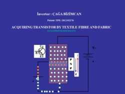 Patent
 Nu : TR 2013/ 02276- Çağa Bizimcan SUMMARY
ACQUIRING TRANSISTOR BY TEXTILE FIBRE AND FABRIC
The invention is to provide voltage and current acquisition by increasing and decreasing electrical current charged the panels in the mobility emerged along with the replacement made by the pressure and the electrons located outer orbit of atoms composed between the panels P-type and N-type triggering each other through the fabric panels knitted and/or weaved with threads composed of the fibres including reinforced N and P type fibres and/or both N and P types crystals and/or the fibres including reinforced crystals directly and/ or N type and P type and/or continuous staple by the electricity acquired through natural and artificial ways or all other chemical ways and petroleum and petroleum-derived along with all kind of renewable energy resources especially solar power.
INSTRUCTION
ACQUIRING TRANSISTOR BY TEXTILE FIBRE AND FABRIC
Technical Area
This invention is to provide voltage and current acquisition by increasing electrical current charged semi conductive NPN type and/or PNP type panels occurred the cell and /or cells constituted by means of reinforced processing of the fabrics in known sewing machine and/or making the technique become knitted fabric and textile fabric in weaving looms and/or knitting machine and/or brode and raschel machines through all kind of conductive metals or conductive fibre or thread or conductive metal thread providing transmission of electrical current and (P-type) and (N-Type) fibres produces within the scope of the invention and/or transistor production providing voltage and current acquisition by increasing electrical current with the threads produced by merging fibre and two and more fibres produced by being doped through saturating and/or doping and/or harmonizing with the elements especially boron with atomic number 5 and phosphorus with atomic number 15 within 3. And 5 group of periodic table by undergoing various chemical process on relatively thin industrial glass called barium aluminoborosilicate and/or derivatives of barium and aluminium element and silicium-boron mixture or Germanium and/or compounds or other all kind of continuous and/or discontinuous fibres with (P-type) and (N-Type) threads produced from silicon and/or glass fibre or fibres up to the highest denier starting from normal or crystallized silicon thread or fibre and/or normal or crystallized glass fibre or thread or glass wool continuous or discontinuous normal or crystallized 3. group silicon (P-type) and continuous or discontinuous normal or crystallized 5. group silicon (N-Type) nano scale acquired by harmonising or being doped of the compound chemical additive elements and/or 3. Group and 5. Group elements of periodic table related to mono crystallized or crystallized pure silicium or crystallized silicon raw material and/or mono crystallized or crystallized Germanium and/or mono crystallized or crystallized glass raw material within the scope of this invention regarding the electricity acquired through natural and artificial ways or all other chemical ways and petroleum and petroleum-derived along with all kind of renewable energy resources.
In the technical area, in order to increase the conductivity of semi conductive at an ideal and convenient temperature, (P-Type) and (N-Type) semi conductive should be doped with relatively low level – a few ppm - of foreign substance (boron and phosphorus or other elements in the 3rd and 5th group of periodic table) creating gap – holl. As a result of doping this semi conductive, in case semi conductive was being doped by some of silicium or germanium within the crystallized form, atoms of this semi conductive has been replaced by foreign atoms. The process made on these spaces in which the crystallized order of semi conductive is corrupted is called doping. When a semi conductive being doped with a foreign substance creating gap – holl is exposed to voltage as heat, light, power etc externally, and number of free electrons increases highly compared to the situation within the crystal. If the number of free electrons increases through doping, it is called N-type doping; if the number of free electrons decreases and the number of holes increases, then it is called P-type doping. Either N-type or P-type doping, semi conductive being doped by these foreign substances are called as doping semi conductive. Through producing Silicium or Germanium or additive substances composed of other semi conductive and N-type and P-type semi conductive fibres and threads composed of them technically, by producing NPN type or PNP type semi conductive panels, acquisition of voltage and current can be provided by increasing electricity current charged to these panels.
Former Technique
In case the technique is known, in order to increase all kind and power of electrical current and provide voltage acquisition, apart from (P-Type) and (N-type) Fabric panels produced by fibres and threads within the scope of this invention, other semi conductive being doped by other method and techniques and solid type transistor up to about 100.000 kinds have been produced and used in the industry.
Purpose of Invention
The problem which was tried to solve by this invention is the production of textile based transistor directed towards providing voltage and current acquisition by increasing and decreasing electrical current charged the panels in the mobility emerged along with the replacement made by the pressure and the electrons located outer orbit of atoms composed between the panels P-type and N-type triggering each other through the fabric panels knitted and/or weaved with threads composed of the fibres including reinforced N and P type fibres and/or both N and P types crystals and/or the fibres including reinforced crystals directly and/ or N type and P type and/or continuous staple by the electricity acquired through natural and artificial ways or all other chemical ways and petroleum and petroleum-derived along with all kind of renewable energy resources especially solar power.
Explanation of Figures
The fibres and fabrics and/or all kind of textile knitted by the threads composed through these fibres and/or N-Type and P-Type fibres have been indicated in the figures attached for providing acquisition of voltage and current by increasing electricity current charged to the panels composed of the fibres and additive fibres in order to reach the purpose of this invention.
Figure 1: The model explaining the logic of the process of NPN type transistor produced by conductive metal fibres and N-type and P-Type fibres used within the scope of this invention and transistors made by the substances produced apart from the invention and used.
Figure 2: Scheme showing the movement direction of the electricity being charged and the fibre composed of semi conductive fibre being doped in NPN type.
Figure 3: Bending N and P type fibres in the order of NPN.
Figure 4: NPN type tartan Fabric Panel transistor covered by an isolator substance.
Figure 5: NPN type Fabric Panel transistor covered by an isolator substance.
Figure 6: The model explaining the logic of the process of PNP type transistor produced by conductive metal fibres and N-type and P-Type fibres used within the scope of this invention and transistors made by the substances produced apart from the invention and used
Figure 7: Scheme showing the movement direction of the electricity being charged and the fibre composed of semi conductive fibre being doped in PNP type.
Figure 8: Bending N and P type fibres in the order of PNP
Figure 9 : PNP type tartan Fabric Panel transistor covered by an isolator substance.
Figure 10: PNP type Fabric Panel transistor covered by an isolator substance.
Explanation of Figures’ References
1.: N-Type semi conductive fibre. (collector)
2.: P-Type semi conductive fibre.(Base)
3.: N-Type Semi conductive fibre.(Emitter)
4.: The thread composed by bringing N and P type fibres together or bending.
5- Covering outer surface of fibre or threads with an isolator substance
6- : N-Type semi conductive fibre (collector)
7- : P-Type semi conductive fibre.(Base)
8- : N-Type semi conductive fibre. (Emitter)
9- : Warp weft directed sequence of P-Type semi conductive fibres on textile fabric (Base)
10- : Warp weft directed sequence of N-Type semi conductive fibres on textile fabric
11- : Warp weft directed sequence of conductive metal fibres on textile fabric or its aspect embroidered
12- : Warp weft directed sequence of isolator fibres on textile fabric
13- : Electrical current charging key
14- : P-Type sub fibre group sequence in PNP type transistor (Collector)
15- : N-Type middle fibre group sequence in PNP type transistor (Base)
16- : P-Type upper fibre group sequence in PNP type transistor (Emitter)
17- : Covering PNP type transistor group with isolator substance
18- : P-Type sub fibre group bending in PNP type transistor (Collector)
19- : N-Type middle fibre group bending in PNP type transistor (Base)
20- : P-Type upper fibre group bending in PNP type transistor (Emitter)
21- : Covering PNP type twisted transistor group with isolator substance
22- : Distribution channel through the metal fibre or wire in which the electricity current passing
23- : The area knitted or weaved by isolator fibre surrounding fabric panel
24- : Warp weft directed sequence of P-Type semi conductive fibres on textile fabric
25- : Warp weft directed sequence of N-Type semi conductive fibres on textile fabric
26- : Weaving or embroidering PNP type transistor fabric panel providing the transmission of electrical current
27- : Covering PNP type twisted transistor group with isolator substance
28 : Processing metal fibres or wires through weaving and/or embroidering.
Explanation of Invention:
A- The invention is a textile based transistor device directed towards providing voltage and current acquisition by increasing electrical current charged semi conductive NPN type and/or PNP type panels occurred the cell and /or cells constituted by means of reinforced processing of the fabrics in known sewing machine and/or making the technique become knitted fabric and textile fabric in weaving looms and/or knitting machine and/or brode and raschel machines through all kind of conductive metals or conductive fibre or thread or conductive metal thread providing transmission of electrical current and (P-type) and (N-Type) fibres produces within the scope of the invention and/or transistor production providing voltage and current acquisition by increasing electrical current with the threads produced by merging fibre and two and more fibres produced by being doped through saturating and/or doping and/or harmonizing with the elements especially boron with atomic number 5 and phosphorus with atomic number 15 within 13. and 15 group of periodic table by undergoing various chemical process on relatively thin industrial glass called barium aluminoborosilicate and/or derivatives of barium and aluminium element and silicium-boron mixture or Germanium and/or compounds or other all kind of continuous and/or discontinuous fibres with (P-type) and (N-Type) threads produced from silicon and/or glass fibre or fibres up to the highest denier starting from normal or crystallized silicon thread or fibre and/or normal or crystallized glass fibre or thread or glass wool continuous or discontinuous normal or crystallized 3. group silicon (P-type) and continuous or discontinuous normal or crystallized 5. group silicon (N-Type) nano scale acquired by harmonising or being doped of the compound chemical additive elements and/or 3. Group and 5. Group elements of periodic table related to mono crystallized or crystallized pure silicium or crystallized silicon raw material and/or mono crystallized or crystallized Germanium and/or mono crystallized or crystallized glass raw material.
B-The invention is textile based transistor device covered its outer surface by isolator case directed towards providing voltage and current acquisition by increasing and decreasing electrical current charged the panels in the mobility emerged along with the replacement made by the pressure and the electrons located outer orbit of atoms composed between the panels P-type and N-type triggering each other through the fabric panels knitted and/or weaved with threads composed of the fibres including reinforced N and P type fibres and/or both N and P types crystals and/or the fibres including reinforced crystals directly and/ or N type and P type and/or continuous staple by the electricity acquired through natural and artificial ways or all other chemical ways and petroleum and petroleum-derived along with all kind of renewable energy resources especially solar power.
C- Functioning of NPN type transistor produced by N-Type and P-Type fire or threads is as follows. Formation of NPN type transistor compose of a base substance constituted two N type semi conductive fibres and threads and P type semi conductive fibre and thread located between them as a thin layer. Base layer located between two N type fibre and threads functions for controlling electronic transition. The textile based transistor may enlarge small currents or may ensure a huge receiver functioning with a small current by supervising the current transiting. As it is seen in Figure 1, in NPN type transistors, while anode of Vbb resource charged base pole positively, cathode of Vss resource pushes the electrons in the emitter pole up. The electrons pressed have been pulled by the base. Electrons in the transmittal line of the emitter enter into the base region by exceeding E-B voltage set, however, while about 2-3 % of the electrons coming from emitter region have been pulled by base region due to narrowness of base region, remaining 97-98 % passed to the collector. Anode of Vcc resource pulls the electrons toward collector region and electron flow become continuous and electron flow from emitter to collector continues as long as the base low given by Vbb resource continues. Electrons go up, holes go down in NPN type transistors and therefore, positive signal implemented to the base passes current from collector towards the emitter. It is known that emitter flow is equal to the sum of base and collector flows.
D- Form of PNP type transistor produces with P-type and N-Type fibre or threads is the same as NPN type transistor. The difference is to locate N type semi conductive fibre and thread between two P type semi conductive fibres and threads as a thin layer. In PNP type transistors, while cathode of Vbb resource charged base pole negatively, anode of Vcc resource pushes the holes charged positively in the emitter pole up. By this way, the ones positively charged and pressed have been pulled by the base and passed towards the collector region. The movement of holes become continuous since cathode of Vcc resource pull the holes in the collector region itself. This movement towards the collector continues as long as the Vbb flow continues. Electrons go down, holes go up in PNP type transistors and therefore, negative signal implemented to the base transmits current from emitter towards the collector. It is also known that emitter flow is equal to the sum of base and collector flows.
Implementation Style of Invention to Industry
The above-mentioned purposes, the electricity produced all kinds of respect for the environment and nature of the invention is safe and additive fibres and the fibres of the panels and install the electric current by increasing the acquisition of voltage and current of the textile based transistor enables this device to ensure easy and safe and it is possible to mount the electronic devices compactly that this product can be obtained and abundant raw materials are those known in nature. The product can be produced in the sector of industry especially in textile and energy and/or any other branch of the industry and can be used in every field and applicable in industry.
REQUETS
1)Invention is(P-Type) fibre production method and its qualification is; to subject the process of production of continuous or discontinuous (P-Type) fibres in the machines known as the technique for producing textile fibre of semi conductive mono crystallized or crystallized silicium with single or multiple crystals or silicon substance and/or mono crystallized or crystallized glass substance or all other semi conductive elements in periodic table and/or compounds and pure or compound elements from the 3rd group of periodic table (boron, aluminium, gallium, indium, thallium, unutrium, holmium, einsteinium) being doped starting from nano scale to the highest thickness.
2)It is the method characteristics in Request 1; By bringing 2 or more (P-Type) fibres together, to start with the smallest number of similar fibre types and/or nano scaled numbers, to include textile based fibre up to the highest number.
3) Invention is (P-Type) fibre production method and its qualification is; to subject the process of production of continuous or discontinuous type (P-Type) fibres in the machines producing textile fibre known as the technique up to the highest thickness starting from nano scale with one or more doping mono crystallized or crystallized germanium element and pure or compound gallium element from 3rd group of periodic table.
4)It is the method characteristics in Request 3; By bringing 2 or more (P-Type) fibres together, to start with the smallest number of similar fibre types and/or nano scaled numbers, to include textile based fibre up to the highest number.
5) Invention is (N-Type) fibre production method and its qualification is; to subject the process of production of continuous or discontinuous (N-Type) fibres in the machines known as the technique for producing textile fibre of semi conductive mono crystallized or crystallized silicium with single or multiple crystals or silicon substance and/or mono crystallized or crystallized glass substance or all other semi conductive elements in periodic table and/or compounds and pure or compound elements from the 5th group of periodic table (Nitrogen, phosphorus, arsenic, antimony, bismuth, ununpentium) or mono crystallized or crystallized Germanium element with the element Lithium from … group of periodic table being doped starting from nano scale up to the highest thicknes
6)It is the method characteristics in Request 5; By bringing 2 or more (N-Type) fibres together, to start with the smallest number of similar fibre types and/or nano scaled numbers, to include textile based fibre up to the highest number
7)Invention is (N-Type) fibre production method and its qualification is; to subject the process of production of continuous or discontinuous type (N-Type) fibres in the machines producing textile fibre known as the technique up to the highest thickness starting from nano scale with one or more doping mono crystallized or crystallized germanium element and pure or compound other element from 5th group of periodic table.
It is the method characteristics in Request 7; By bringing 2 or more (N-Type) fibres together, to start with the smallest number of similar fibre types and/or nano scaled numbers, to include textile based fibre up to the highest number.
9) The request is the NPN type textile thread based production method and its characteristics; As it is in the model of Figure 1, by model as in claim 5 and 7, obtained by process step (n-type) two or more twisted fibres among themselves so that the innermost (5) and / or untwisted (1) by treatment assemble and this istem1'deki on fibres obtained by processing steps (P-type) two or more fibres, (n-type) fibres twisted (6) or untwisted (2) wound on any processing and which forms the middle layer (P-type) fibres so that the (n-type) two or more fibres twisted (7) and / or untwisted (3) to be wound on the top as in Figure 2 and Figure 3, by treatment, as in the n-type semi-conductive fibre made of such transactions.
(collector) (1), (n-type) semiconductor fibre (emitter) (3) arrangement of fibres arranged in a layer between the p-type semiconductor thin fibres (the base) (2) consisting of the series base thereof and the outer surface of the whole insulator assembly coated with the substance (4), (8) consists of NPN type transistor thread. NPN type transistor arrangement of fibres between the two N-type, P-type layer of fibres base (2) to control the passage of electrons through the task of the present invention, the transistor is produced in the form of textile yarn based on his business, or a small current by checking the amplification of small currents is that the operation of a receiver with a large current.
10) It is the method characteristics in Request 9; Nano-scale in request 9 to a thickness of the highest starting NPN type transistor-based fibres produced (the base), which forms the P-type fibres (+). (Emitter) constituting the yarn wrapped on top of the N-type fibres (-) poles are connected to the bottom of the wrapped yarn with a given electric charge and the thread (collector) portion of the fibres forming the n-type electron structure by compressing the electricity base in small (+) flows increased by enlarging the (+) supply current, and the thread is no fibre without the burden of poles connected directly to the electrical current sent to the (-) currents amplified by the device (+) flows and loads to be exported as a result of a merger in the end the work is to provide a great receiver. (Figure:1-Figure:2)
11) The request is the production method textile thread based PNP type transistor and its characteristics; As in the model of Figure 6, obtained by the processing steps of claim 1 and 3 (P-type) two or more filaments twisted with each other so that the innermost (19) and / or untwisted (15) by treatment of a and commencing upon claim 5, wherein the fibres obtained by the process steps (n-type) two or more fibres (P-type) fibres twisted (20) or untwisted (16) wound on the middle layer formed and any processing of the (n-type) so that the fibres on (P-type) of 2 or more twisted fibres (21) and / or untwisted (17) to be wound on the top as in Figure 6 and in Figure 7 by treatment as with the P-type semiconductor fibre such transactions. (collector) (15), (P-type) semiconductor fibre (emitter) (17) between the assembly of fibres arranged in a thin layer of N-type semi-conductive fibres (the base) (16) consisting of the series base thereof and the outer surface of the apparatus coated with the whole non-conductive material (18), (22) is composed of PNP type transistor thread.
12) It is the method characteristics in Request 11; Request 11 to a thickness of the highest starting nano-scale PNP type transistor-based fibres produced (the base) constituting the N-type fibres (-). (Emitter) constituting the yarn wrapped on top of the P-type fibres (+) poles provided with electric charge by connecting the bottom of the yarn and the thread is wrapped (collector) portion of the fibres which constitute the P-type (the base) to the (-) of the load compression electricity with a small (-) flows increased by enlarging the (-) supply current, and the thread is no life without the burden of poles connected directly to the electrical current sent to the (+) currents amplified by the device (-) flows as a result of a large receiver end, the combination of loads and exporting is to work. (Figure:6 -Figure:7)
13 ) It is method mentioned in the requests above and its characteristic; 1,2,3,4,5,6,7,8 claim in Figure to form a NPN type transistor 4 and Figures: 5'deki woven fabrics, as in the N-type semiconductor yarns (collector) (1), N-Type Semiconductor yarn (Emitter) (3) arrangement of the warp and weft yarns of the warp and weft yarns formed into a thin layer between the P-type semiconductor (Base) (2) which consists of yarns of yarn strands. N-type semi conductive weft direction on the woven fabric warp arrangement (10) between the P-type semiconductor warp yarns in the weft direction on the woven fabric (the base) layer (9) formed looms or knitting machines, woven and knitted from yarns of yarn knitted insulator edges (12) and conductive metal wires woven yarn or yarns out of insulator and / or may be processed by embroidery (11) N-type semi conductive on the weft yarns in the warp direction of their formation of woven fabric (10), the N-type semiconductor on the fabric, the weaving direction of weft warp array (12) electron and providing passage over the panels are covered with non-conductive material (27) and by the task of checking of the invention, textile weaving or knitting finished his operation based on the current through the transistor by controlling the growth of a small or a small current flows through the operation of the receiver is that it provides a large current.
14) It is method mentioned in the requests above and its characteristic; 1,2,3,4,5,6,7,8 claim in Figure to form a PNP type transistor: and Figure 9: 10, as well as woven fabrics, yarns, the P-type semi conductive (collector) (15) P-Type Semi conductive yarn (Emitter) (17) set up between the warp and weft yarns of the warp and weft yarns are created in a thin layer of n-type semi-conductor (Base) (16) which consists of yarns composed of fibers. P-type semiconductor on the fabric, the weaving direction of weft warp array (26) between the n-type semi-conductive warp yarns in the weft direction on the woven fabric (the base) layer (25) looms or knitting machines to be formed from woven and knitted yarns edges yarn knitted insulator (24) and insulation of the conductor metal thread or wire woven yarns and / or may be processed by embroidery (28) n-type semi-conductive warp yarns in the weft direction of their formation on the woven fabric (25), the P-type semi conductive yarns woven fabric that on the weft warp array (26) providing passage of electrons and the panels are coated with non-conductive material via (27) and acting as a control of the invention, finished woven or knit based textile current through these transistors work done by controlling the growth or small flows the operation of the receiver is that it provides a large current with a small.  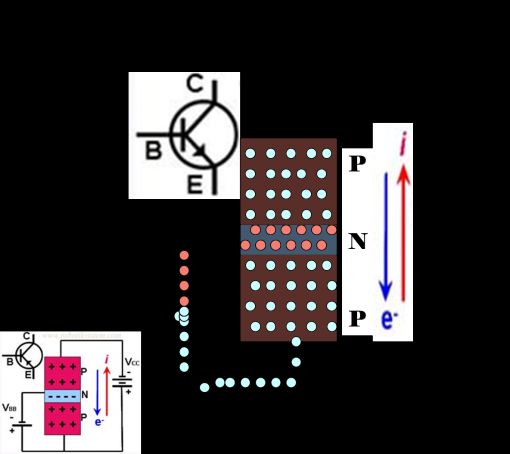 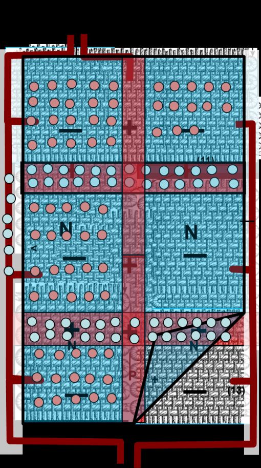 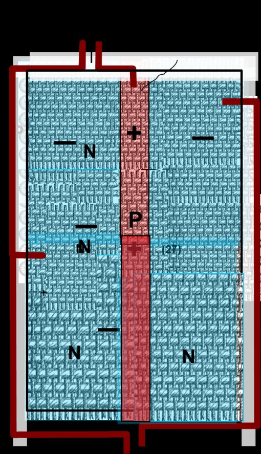 |
|
1800 kez okundu
YorumlarHenüz yorum yapılmamış. İlk yorumu yapmak için tıklayın |